NTD50N03R-1G ON Semiconductor, NTD50N03R-1G Datasheet
NTD50N03R-1G
Specifications of NTD50N03R-1G


Related parts for NTD50N03R-1G

NTD50N03R-1G Summary of contents
Page 1
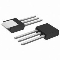
... V N−Channel CASE 369D CASE 369AC DPAK 3 IPAK (Straight Lead) (Straight Lead) STYLE 2 MARKING DIAGRAMS & PIN ASSIGNMENTS 4 Drain 4 Drain Gate Source Drain Source Drain Y = Year WW = Work Week T50N03R = Device Code G = Pb−Free Package ORDERING INFORMATION Publication Order Number: NTD50N03R/D ...
Page 2
... Gate−to−Source Charge Gate−to−Drain Charge 3. Surface−mounted on FR4 board using pad Cu. 4. Surface−mounted on FR4 board using the minimum recommended pad size. 5. Pulse Test: Pulse Width ≤ 300 ms, Duty Cycle ≤ 2%. NTD50N03R (T = 25°C unless otherwise noted) J Symbol ...
Page 3
... Forward Diode Voltage Reverse Recovery Time Charge Time Discharge Time Reverse Recovery Charge PACKAGE PARASITIC VALUES Source Inductance Drain Inductance Gate Inductance Gate Resistance 6. Switching characteristics are independent of operating junction temperatures. NTD50N03R (continued 25°C unless otherwise noted) J Symbol Test Condition t d(on ...
Page 4
... V , GATE−TO−SOURCE VOLTAGE (VOLTS) GS Figure 3. On−Resistance versus Gate−to−Source Voltage 2 1 1.6 1.4 1.2 1.0 0.8 0.6 −50 − JUNCTION TEMPERATURE (°C) J Figure 5. On−Resistance Variation with Temperature NTD50N03R 100 ≥ 0.030 T = 25° 25°C J 0.025 0.020 ...
Page 5
... R , GATE RESISTANCE (W) G Figure 9. Resistive Switching Time Variation versus Gate Resistance 1000 SINGLE PULSE 100 10 1 0.1 Figure 11. Maximum Rated Forward Biased NTD50N03R 25° iss oss 4 C rss Figure 8. Gate−to−Source and Drain−to−Source Voltage versus Total Charge ...
Page 6
... ORDERING INFORMATION Order Number NTD50N03R NTD50N03RG NTD50N03RT4 NTD50N03RT4G NTD50N03R−1 NTD50N03R−1G NTD50N03R−35 NTD50N03R−35G †For information on tape and reel specifications, including part orientation and tape sizes, please refer to our Tape and Reel Packaging Specifications Brochure, BRD8011/D. NTD50N03R P (pk ...
Page 7
... ON Semiconductor Soldering and Mounting Techniques Reference Manual, SOLDERRM/ −T− SEATING K PLANE 0.13 (0.005 NTD50N03R PACKAGE DIMENSIONS DPAK CASE 369C−01 ISSUE O SEATING −T− PLANE SOLDERING FOOTPRINT* 6.20 3.0 0.244 0.118 2.58 0.101 1.6 6.172 0.243 ...
Page 8
... J 0.018 0.023 0.46 0.58 K 0.134 0.142 3.40 3.60 R 0.180 0.215 4.57 5.46 V 0.035 0.050 0.89 1.27 W 0.000 0.010 0.000 0.25 ON Semiconductor Website: http://onsemi.com Order Literature: http://www.onsemi.com/litorder For additional information, please contact your local Sales Representative. NTD50N03R/D ...