NTD78N03-35G ON Semiconductor, NTD78N03-35G Datasheet
NTD78N03-35G
Specifications of NTD78N03-35G


Related parts for NTD78N03-35G


NTD78N03-35G Summary of contents
Page 1
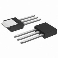
... CASE 369AD CASE 369D IPAK DPAK (Straight Lead) (Straight Lead) STYLE 2 MARKING DIAGRAMS & PIN ASSIGNMENTS 4 Drain 4 4 Drain Gate Drain Source Source Gate Drain Source Y = Year WW = Work Week 78N03 = Device Code G = Pb−Free Package ORDERING INFORMATION Publication Order Number: NTD78N03/D ...
Page 2
... Reverse Recovery Time PACKAGE PARASITIC VALUES Source Inductance Drain Inductance Gate Inductance Gate Resistance 3. Pulse Test: Pulse Width ≤ 300 ms, Duty Cycle ≤ 2%. 4. Switching characteristics are independent of operating junction temperatures. NTD78N03 (T = 25°C unless otherwise noted) J Symbol Test Condition = 250 mA V ...
Page 3
... I , DRAIN CURRENT (A) D Figure 3. On−Resistance versus Drain Current and Temperature 4 2.5 2 1.5 1 0.5 0 −50 − JUNCTION TEMPERATURE (°C) J Figure 5. On−Resistance Variation with Temperature NTD78N03 160 ≥ 150 DS 3.8 V 140 130 3.6 V 120 110 100 3 3 25° 25° 2 Figure 2 ...
Page 4
... SINGLE PULSE T = 25° LIMIT DS(on) THERMAL LIMIT PACKAGE LIMIT 0.1 0 DRAIN−TO−SOURCE VOLTAGE (VOLTS) DS Figure 11. Maximum Rated Forward Biased Safe Operating Area NTD78N03 25° iss 2 C oss Figure 8. Gate−to−Source and Drain−to−Source Voltage versus Total Charge ...
Page 5
... Figure 14. Thermal Response − Various Duty Cycles ORDERING INFORMATION Order Number NTD78N03 NTD78N03G NTD78N03T4 NTD78N03T4G NTD78N03−1 NTD78N03−1G NTD78N03−35 NTD78N03−35G †For information on tape and reel specifications, including part orientation and tape sizes, please refer to our Tape and Reel Packaging Specifications Brochure, BRD8011/D. NTD78N03 di/ ...
Page 6
... 0.13 (0.005) M 5.80 0.228 *For additional information on our Pb−Free strategy and soldering details, please download the ON Semiconductor Soldering and Mounting Techniques Reference Manual, SOLDERRM/D. NTD78N03 PACKAGE DIMENSIONS DPAK (SINGLE GUAGE) CASE 369AA−01 ISSUE A SEATING −T− PLANE SOLDERING FOOTPRINT* 6.20 3 ...
Page 7
... D2 4.80 −−− E 6.35 6.73 E2 4.70 −−− E3 4.45 5.46 e 2.28 BSC D2 L 3.40 3.60 L1 −−− 2.10 L2 0.89 1.27 ON Semiconductor Website: www.onsemi.com Order Literature: http://www.onsemi.com/orderlit For additional information, please contact your local Sales Representative NTD78N03/D ...