NTY100N10 ON Semiconductor, NTY100N10 Datasheet
NTY100N10
Specifications of NTY100N10
Available stocks


Related parts for NTY100N10

NTY100N10 Summary of contents
Page 1
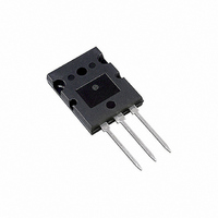
... A, 100 (Typ) GS N−Channel MARKING DIAGRAM & PIN ASSIGNMENT NTY100N10 AYYWWG TO−264 STYLE Assembly Location YY = Year WW = Work Week G = Pb−Free Package ORDERING INFORMATION Package Shipping TO−264 25 Units/Rail TO−264 25 Units/Rail (Pb−Free) Publication Order Number: NTY100N10/D ...
Page 2
ELECTRICAL CHARACTERISTICS Characteristic OFF CHARACTERISTICS Drain−Source Breakdown Voltage ( 250 mA (Positive Temperature Coefficient) Zero Gate Voltage Drain Current ( Vdc 100 Vdc 25° ...
Page 3
9 8 150 100 DRAIN−TO−SOURCE VOLTAGE (V) DS Figure 1. On−Region ...
Page 4
Switching behavior is most easily modeled and predicted by recognizing that the power MOSFET is charge controlled. The lengths of various switching intervals (Dt) are determined by how fast the FET input capacitance can be charged by current from the ...
Page 5
100 1000 t d(off 100 ...
Page 6
The Forward Biased Safe Operating Area curves define the maximum simultaneous drain−to−source voltage and drain current that a transistor can handle safely when it is forward biased. Curves are based upon maximum peak junction temperature and a case temperature (T ...
Page 7
D = 0.5 0.2 0.1 0.05 0.1 0.02 0.01 SINGLE PULSE 0.01 1.0E−05 1.0E− Figure 14. Diode Reverse Recovery Waveform SAFE OPERATING AREA P (pk DUTY CYCLE 1.0E−03 1.0E−02 t, ...
Page 8
... Q 3.1 3.5 0.122 0.137 R 2.25 REF 0.089 REF U 6.3 REF 0.248 REF W 2.8 3.2 0.110 0.125 STYLE 1: PIN 1. GATE 2. DRAIN 3. SOURCE ON Semiconductor Website: http://onsemi.com Order Literature: http://www.onsemi.com/litorder For additional information, please contact your local Sales Representative. NTY100N10/D ...