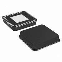
AD5751ACPZ Analog Devices Inc, AD5751ACPZ Datasheet - Page 20

AD5751ACPZ
Manufacturer Part Number
AD5751ACPZ
Description
PLC OUR DRIVER +60V I.C.
Manufacturer
Analog Devices Inc
Datasheet
1.AD5751ACPZ.pdf
(32 pages)
Specifications of AD5751ACPZ
Amplifier Type
Instrumentation
Number Of Circuits
1
Slew Rate
2 V/µs
Current - Supply
5.2mA
Current - Output / Channel
24mA
Voltage - Supply, Single/dual (±)
10.8 V ~ 55 V
Operating Temperature
-40°C ~ 105°C
Mounting Type
Surface Mount
Package / Case
32-LFCSP
No. Of Amplifiers
1
Amplifier Output
Single Ended
Supply Voltage Range
10.8V To 55V
Supply Current
5.2mA
Amplifier Case Style
LFCSP
No. Of Pins
32
Rohs Compliant
Yes
Lead Free Status / RoHS Status
Lead free / RoHS Compliant
Output Type
-
-3db Bandwidth
-
Gain Bandwidth Product
-
Current - Input Bias
-
Voltage - Input Offset
-
Lead Free Status / RoHS Status
Lead free / RoHS Compliant
AD5751
TERMINOLOGY
Total Unadjusted Error (TUE)
TUE is a measure of the output error taking all the various
errors into account: INL error, offset error, gain error, and
output drift over supplies, temperature, and time. TUE is
expressed as a percentage of full-scale range (% FSR).
Relative Accuracy or Integral Nonlinearity (INL)
INL is a measure of the maximum deviation, in % FSR, from a
straight line passing through the endpoints of the output driver
transfer function. A typical INL vs. input voltage plot is shown
in Figure 5.
Full-Scale Error
Full-scale error is the deviation of the actual full-scale analog
output from the ideal full-scale output. Full-scale error is
expressed as a percentage of full-scale range (% FSR).
Full-Scale TC
Full-scale TC is a measure of the change in the full-scale error
with a change in temperature. It is expressed in ppm FSR/°C.
Gain Error
Gain error is a measure of the span error of the output. It is the
deviation in slope of the output transfer characteristic from the
ideal expressed in % FSR. A plot of gain error vs. temperature is
shown in Figure 10.
Gain Error TC
Gain error TC is a measure of the change in gain error with
changes in temperature. Gain error TC is expressed in ppm
FSR/°C.
Zero-Scale Error
Zero-scale error is the deviation of the actual zero-scale analog
output from the ideal zero-scale output. Zero-scale error is
expressed in millivolts (mV).
Rev. A | Page 20 of 32
Zero-Scale TC
Zero-scale TC is a measure of the change in zero-scale error
with a change in temperature. Zero-scale error TC is expressed
in ppm FSR/°C.
Offset Error
Offset error is a measurement of the difference between the
actual VOUT and the ideal VOUT expressed in millivolts (mV)
in the linear region of the transfer function. It can be negative
or positive.
Output Voltage Settling Time
Output voltage settling time is the amount of time it takes for
the output to settle to a specified level for a half-scale input change.
Slew Rate
The slew rate of a device is a limitation in the rate of change of
the output voltage. The output slewing speed is usually limited
by the slew rate of the amplifier used at its output. Slew rate is
measured from 10% to 90% of the output signal and is
expressed in V/μs.
Current Loop Voltage Compliance
Current loop voltage compliance is the maximum voltage at the
IOUT pin for which the output current is equal to the
programmed value.
Power-On Glitch Energy
Power-on glitch energy is the impulse injected into the analog
output when the AD5751 is powered on. It is specified as the
area of the glitch in nV-sec.
Power Supply Rejection Ratio (PSRR)
PSRR indicates how the output is affected by changes in the
power supply voltage.


