BAP70-02,115 NXP Semiconductors, BAP70-02,115 Datasheet - Page 2
BAP70-02,115
Manufacturer Part Number
BAP70-02,115
Description
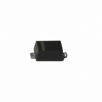
DIODE PIN 50V 100MA SOD-523
Manufacturer
NXP Semiconductors
Datasheet
1.BAP70-02115.pdf
(6 pages)
Specifications of BAP70-02,115
Package / Case
SC-79, SOD-523
Diode Type
PIN - Single
Voltage - Peak Reverse (max)
50V
Current - Max
100mA
Capacitance @ Vr, F
0.25pF @ 20V, 1MHz
Resistance @ If, F
1.9 Ohm @ 100mA, 100MHz
Power Dissipation (max)
415mW
Configuration
Single
Reverse Voltage
50 V
Forward Continuous Current
100 mA
Frequency Range
VHF
Carrier Life
1.25 us
Forward Voltage Drop
1.1 V at 50 mA
Maximum Diode Capacitance
0.25 pF at 20 V
Maximum Operating Temperature
+ 150 C
Maximum Series Resistance @ Maximum If
1.9 Ohms at 100 mA
Maximum Series Resistance @ Minimum If
100 Ohms at 0.5 mA
Minimum Operating Temperature
- 65 C
Mounting Style
SMD/SMT
Power Dissipation
415 mW
Lead Free Status / RoHS Status
Lead free / RoHS Compliant
Other names
568-1940-2
934056619115
BAP70-02 T/R
934056619115
BAP70-02 T/R
Available stocks
Company
Part Number
Manufacturer
Quantity
Price

Part Number:
BAP70-02,115
Manufacturer:
NXP/恩智浦
Quantity:
20 000


NXP Semiconductors
FEATURES
APPLICATIONS
DESCRIPTION
Planar PIN diode in a SOD523 ultra small SMD plastic
package.
LIMITING VALUES
In accordance with the Absolute Maximum Rating System (IEC 60134).
ELECTRICAL CHARACTERISTICS
T
V
I
P
T
T
V
I
C
r
L
j
SYMBOL
F
SYMBOL
R
D
L
S
High voltage, current controlled RF resistor for
attenuators
Low diode capacitance
Very low series inductance.
RF attenuators
(SAT)TV
Car radio.
stg
j
R
tot
= 25 C unless otherwise specified.
F
Silicon PIN diode
d
continuous reverse voltage
continuous forward current
total power dissipation
storage temperature
junction temperature
forward voltage
reverse leakage current
diode capacitance
diode forward resistance
charge carrier life time
series inductance
PARAMETER
PARAMETER
Rev. 05 - 2 January 2008
T
I
V
V
V
V
V
I
I
I
I
when switched from I
I
measured at I
I
F
F
F
F
F
R
F
s
R
R
R
R
R
= 50 mA
= 0.5 mA; f = 100 MHz
= 1 mA; f = 100 MHz
= 10 mA; f = 100 MHz
= 100 mA; f = 100 MHz
= 100 mA; f = 100 MHz
= 6 mA; R
= 90 C
= 50 V
= 0 V; f = 1 MHz
= 1 V; f = 1 MHz
= 5 V; f = 1 MHz
= 20 V; f = 1 MHz
CONDITIONS
PINNING
handbook, halfpage
CONDITIONS
L
R
Marking code: K8.
= 100 ;
= 3 mA
Fig.1 Simplified outline (SOD523) and symbol.
F
= 10 mA to
PIN
1
2
1
T op view
0.9
570
400
270
200
77
40
5.4
1.4
1.25
0.6
TYP.
2
cathode
anode
65
65
MIN.
MAM405
Product specification
DESCRIPTION
1.1
100
250
100
50
7
1.9
MAX.
50
100
415
+150
+150
BAP70-02
MAX.
V
nA
fF
fF
fF
fF
nH
2 of 6
V
mA
mW
s
C
C
UNIT
UNIT
Related parts for BAP70-02,115
Image
Part Number
Description
Manufacturer
Datasheet
Request
R

Part Number:
Description:
Planar PIN diode in a SOD523 ultra small SMD plastic package
Manufacturer:
NXP Semiconductors
Datasheet:

Part Number:
Description:
Bap70-02 Silicon Pin Diode
Manufacturer:
NXP Semiconductors
Datasheet:

Part Number:
Description:
Manufacturer:
NXP Semiconductors
Datasheet:

Part Number:
Description:
DIODE PIN 50V 100MA SOD-323
Manufacturer:
NXP Semiconductors
Datasheet:

Part Number:
Description:
DIODE PIN 50V 100MA SOT-23
Manufacturer:
NXP Semiconductors
Datasheet:

Part Number:
Description:
Planar PIN diode in a SOD323 (SC-76) small SMD plastic package
Manufacturer:
NXP Semiconductors
Datasheet:

Part Number:
Description:
Two planar PIN diodes in series configuration in a SOT323 small SMD plastic package
Manufacturer:
NXP Semiconductors
Datasheet:

Part Number:
Description:
Two planar PIN diodes in common cathode configuration in a SOT23 small SMD plastic package
Manufacturer:
NXP Semiconductors
Datasheet:
Part Number:
Description:
Bap70-03 Silicon Pin Diode
Manufacturer:
NXP Semiconductors
Datasheet:
Part Number:
Description:
Manufacturer:
NXP Semiconductors
Datasheet:
Part Number:
Description:
Silicon PIN Diode
Manufacturer:
NXP Semiconductors
Datasheet:

Part Number:
Description:
Silicon PIN diode - C<sub>d</sub> typ.: 0.25@VR=20V AND F=1MHz max0.40@VR=1V and F=1MHz0.57@VR=0V and F=1MHz pF; Configuration: Single ; I<sub>F</sub> max: 100 mA; R<sub>D</sub> @ I<sub>F</sub>=0.5 mA A
Manufacturer:
NXP Semiconductors / Philips Semiconductors
Part Number:
Description:
Silicon PIN diode - C<sub>d</sub> typ.: 0.25@VR=20V AND F=1MHz max0.40@VR=1V and F=1MHz0.57@VR=0V and F=1MHz pF; Configuration: Single ; I<sub>F</sub> max: 100 mA; R<sub>D</sub> @ I<sub>F</sub>=0.5 mA A
Manufacturer:
NXP Semiconductors / Philips Semiconductors
Part Number:
Description:
Silicon PIN diode - C<sub>d</sub> typ.: 0.25@VR=20V and F=1MHz0.43@VR=1V and F=1MHz0.6@VR=0V and F=1MHz pF; Configuration: Common cathode ; I<sub>F</sub> max: 100 mA; R<sub>D</sub> @ I<sub>F</sub>=0.5 m
Manufacturer:
NXP Semiconductors / Philips Semiconductors