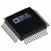
AD1835AASZ Analog Devices Inc, AD1835AASZ Datasheet - Page 12

AD1835AASZ
Manufacturer Part Number
AD1835AASZ
Description
Audio Codec 2ADC / 8DAC 24-Bit 52-Pin MQFP
Manufacturer
Analog Devices Inc
Type
General Purposer
Datasheet
1.AD1835AASZ.pdf
(24 pages)
Specifications of AD1835AASZ
Package
52MQFP
Adc/dac Resolution
24 Bit
Number Of Channels
2ADC /8 DAC
Sampling Rate
96 KSPS
Number Of Adcs
2
Number Of Dacs
8
Operating Supply Voltage
3.3|5 V
Data Interface
Serial
Resolution (bits)
24 b
Number Of Adcs / Dacs
2 / 8
Sigma Delta
Yes
S/n Ratio, Adcs / Dacs (db) Typ
105 / 108
Dynamic Range, Adcs / Dacs (db) Typ
105 / 108
Voltage - Supply, Analog
4.5 V ~ 5.5 V
Voltage - Supply, Digital
4.5 V ~ 5.5 V
Operating Temperature
-40°C ~ 85°C
Mounting Type
Surface Mount
Package / Case
52-BQFP
Lead Free Status / RoHS Status
Lead free / RoHS Compliant
For Use With
EVAL-AD1835AEB - BOARD EVALUATION FOR AD1835A
Lead Free Status / RoHS Status
Lead free / RoHS Compliant
Available stocks
Company
Part Number
Manufacturer
Quantity
Price
Company:
Part Number:
AD1835AASZ
Manufacturer:
ADI
Quantity:
30
Company:
Part Number:
AD1835AASZ
Manufacturer:
Analog Devices Inc
Quantity:
10 000
Company:
Part Number:
AD1835AASZ-REEL
Manufacturer:
Analog Devices Inc
Quantity:
10 000
AD1835A
Sample Rate
IMCLK/512
IMCLK/256
To maintain the highest performance possible, the clock jitter of
the master clock signal should be limited to less than 300 ps
rms, measured using the edge-to-edge technique. Even at these
levels, extra noise or tones may appear in the DAC outputs if
the jitter spectrum contains large spectral peaks. It is highly
recommended that the master clock be generated by an inde-
pendent crystal oscillator. In addition, it is especially important
that the clock signal not be passed through an FPGA or other
large digital chip before being applied to the AD1835A. In most
cases, this will induce clock jitter due to the fact that the clock
signal is sharing common power and ground connections with
unrelated digital output signals.
RESET and Power-Down
PD/RST will power down the chip and set the control registers
to their default settings. After PD/RST is de-asserted, an
initialization routine will run inside the AD1835A to clear all
memories to zero. This initialization lasts approximately 20
LRCLK intervals. During this time, it is recommended that no
SPI writes occur.
MCLK
12.288MHz
CLATCH
COUT
CCLK
Table III. ADC Sample Rate Settings
CIN
t
COE
t
CLS
D15
CLOCK SCALING
t
CCP
ADC Control 1 Register
1100000xx0xxxxxx (48 kHz)
1100000xx1xxxxxx (96 kHz)
ADC O/P
DAC I/P
D14
2/3
1
2
48kHz/96kHz/192kHz
48kHz/96kHz
Figure 2. Modulator Clocking Scheme
t
COD
Figure 3. Format of SPI Timing
D9
D9
t
CCH
t
CDS
t
IMCLK = 24.576MHz
CCL
D8
D8
t
CDH
INTERPOLATION
–12–
OPTIONAL
FILTER
HPF
Power Supply and Voltage Reference
The AD1835A is designed for 5 V supplies. Separate power supply
pins are provided for the analog and digital sections. These pins
should be bypassed with 100 nF ceramic chip capacitors, as
close to the pins as possible, to minimize noise pickup. A bulk
aluminum electrolytic capacitor of at least 22 F should also be
provided on the same PC board as the codec. For critical applica-
tions, improved performance will be obtained with separate
supplies for the analog and digital sections. If this is not pos-
sible, it is recommended that the analog and digital supplies be
isolated by two ferrite beads in series with the bypass capacitor
of each supply. It is important that the analog supply be as clean
as possible.
The internal voltage reference is brought out on the FILTR pin
and should be bypassed as close as possible to the chip, with a
parallel combination of 10 µF and 100 nF. The reference volt-
age may be used to bias external op amps to the common-mode
voltage of the analog input and output signal pins. The current
drawn from the V
Serial Control Port
The AD1835A has an SPI compatible control port to permit
programming the internal control registers for the ADCs and
DACs and for reading the ADC signal levels from the internal
peak detectors. The SPI control port is a 4-wire serial control port.
DECIMATOR /
ADC ENGINE
DAC ENGINE
MODULATOR
FILTER
Σ-∆
REF
pin should be limited to less than 50 A.
MODULATOR
DAC
Σ-∆
D0
D0
t
CLH
t
COTS
ANALOG
OUTPUT
ANALOG
INPUT
REV. A


