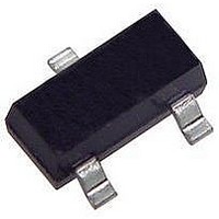
HSMS-286E-BLKG Avago Technologies US Inc., HSMS-286E-BLKG Datasheet

HSMS-286E-BLKG
Specifications of HSMS-286E-BLKG
Related parts for HSMS-286E-BLKG
HSMS-286E-BLKG Summary of contents
Page 1
... Unique Configurations in Surface Mount SOT‑363 Package – increase flexibility – save board space – reduce cost • HSMS‑286K Grounded Center Leads Provide Higher Isolation • Matched Diodes for Consistent Performance • Better Thermal Conductivity for Higher Power Dissipation • ...
Page 2
... T4 4 2865 T5 5 Test Conditions Notes: 1. ∆VF for diodes in pairs is 15.0 mV maximum at 1.0 mA. 2. ∆CT for diodes in pairs is 0.05 pF maximum at –0.5V. SOT-323/SOT-363 DC Electrical Specifications, T Part Package Number Marking Lead HSMS- Code Code 286B T0 B 286C T2 C 286E T3 E 286F T4 F 286K ...
Page 3
... RF Electrical Specifications +25°C, Single Diode C Part Typical Tangential Sensitivity Number TSS (dBm HSMS- 915 MHz 2.45 GHz 2860 – 57 –56 2862 2863 2864 2865 286B 286C 286E 286F 286K 286L 286P 286R Test Video Bandwidth = 2 MHz Conditions µA b Absolute Maximum Ratings +25° ...
Page 4
... where I = externally applied bias current in amps saturation current (see table of SPICE parameters temperature, ° ideality factor (see table of SPICE parameters) Note: To effectively model the packaged HSMS-286x product, please refer to Application Note AN1124. 4 SPICE Parameters Parameter Units Value ‑ 5 ...
Page 5
Typical Parameters, Single Diode 100 –55° +25° +85° .01 0.1 0.2 0.3 0.4 0.5 0 0.8 0.9 1.0 FORWARD VOLTAGE ( 100 ...
Page 6
... In small signal detector applications (P < ‑20 dBm), this diode is in used with DC bias at frequencies above 1.5 GHz. At lower frequencies, the zero bias HSMS‑285x family should be considered. In large signal power or gain control applications (P > ‑20 dBm), this family is used without bias at in frequencies above 4 GHz ...
Page 7
... These circuits can take a variety of forms, but in the most simple case they appear as shown in Figure 9. This is the basic detector circuit used with the HSMS‑ 286x family of diodes. Output voltage can be virtually doubled and input impedance (normally very high) can be halved through ...
Page 8
... DIMENSIONS ARE FOR MICROSTRIP ON 0.032" THICK FR-4. Figure 11. 915 MHz Matching Network for the HSMS-286x Series at 3 µA Bias inductor rotates the impedance of the diode to a point on the Smith Chart where a shunt inductor can pull the center. The short length of 0.065” wide HSMS-285A/6A fig 14 microstrip line is used to mount the lead of the diode’ ...
Page 9
... Figure 17 is much less sensitive to changes in diode and circuit board processing. 5.8 GHz Detector Circuit A possible design for a 5.8 GHz detector is given in Figure 21. RF INPUT Figure 21. 5.8 GHz Matching Network for the HSMS-286x Series at 3 µA Bias. 2.45 2.6 FREQUENCY (GHz) HSMS-285X fig 24 was 21 VIDEO OUT WIDTH = 0.016" ...
Page 10
... RF impedance. A glance at Figure 6 suggests that the 5.9 6.0 proper choice of bias current in the HSMS‑286x series can minimize variation over temperature. The detector circuits described earlier were tested over temperature. The 915 MHz voltage doubler using the HSMS‑ ...
Page 11
... This is best achieved by using two diodes single package, such as the SOT‑143 HSMS‑2865 as shown in Figure 29. In high power differential detectors, RF coupling from the detector diode to the reference diode produces a rectified voltage in the latter, resulting in errors. ...
Page 12
... The line marked “RF diode, V ” is the transfer curve for out the detector diode — both the HSMS‑2825 and the HSMS‑ 282K exhibited the same output voltage. The data were taken over the 50 dB dynamic range shown. To the right is the output voltage (transfer) curve for the reference diode of the HSMS‑ ...
Page 13
Diode Burnout Any Schottky junction diode or the gate of a MESFET, is relatively delicate and can be burned out with excessive RF power. Many crystal video receivers used in RFID (tag) applications find themselves in ...
Page 14
SMT Assembly Reliable assembly of surface mount components is a complex process that involves many material, process, and equipment factors, including: method of heating (e.g vapor phase reflow, wave soldering, etc.) circuit board material, conductor thickness and pattern, ...
Page 15
Package Dimensions Outline 23 (SOT-23 XXX SYMBOL Notes: e2 XXX-package marking E Drawings are not to scale L Outline 143 (SOT-143 ...
Page 16
Device Orientation REEL CARRIER TAPE USER FEED DIRECTION COVER TAPE For Outline SOT-143 TOP VIEW ABC ABC ABC ABC Note: "AB" represents package marking code. "C" represents date code. 16 For Outlines SOT-23, -323 8 mm ...
Page 17
Tape Dimensions and Product Orientation For Outline SOT- 9° MAX A 0 DESCRIPTION SYMBOL CAVITY LENGTH A 0 WIDTH B 0 DEPTH K 0 PITCH P BOTTOM HOLE DIAMETER D 1 PERFORATION DIAMETER D PITCH ...
Page 18
... HSMS‑286x‑BLKG 100 where for HSMS‑286x. For product information and a complete list of distributors, please go to our web site: Avago, Avago Technologies, and the A logo are trademarks of Avago Technologies in the United States and other countries. Data subject to change. Copyright © 2005-2009 Avago Technologies. All rights reserved. Obsoletes 5989-4023EN ...


