HSMP-386J-TR1G Avago Technologies US Inc., HSMP-386J-TR1G Datasheet

DIODE PIN SWITCH 100V QFN 2X2

HSMP-386J-TR1G

Manufacturer Part Number
HSMP-386J-TR1G
Description
DIODE PIN SWITCH 100V QFN 2X2
Manufacturer
Avago Technologies US Inc.
Datasheet

Specifications of HSMP-386J-TR1G

Package / Case
8-QFN
Diode Type
Pin - 4 Pair Parallel
Voltage - Peak Reverse (max)
100V
Current - Max
1A
Capacitance @ Vr, F
1.25pF @ 50V, 1MHz
Resistance @ If, F
770 mOhm @ 50mA, 100MHz
Power Dissipation (max)
2W
Configuration
Octal
Reverse Voltage
100 V
Forward Continuous Current
1000 mA
Carrier Life
0.26 us
Maximum Diode Capacitance
1.25 pF @ 50 V
Maximum Operating Temperature
+ 150 C
Maximum Series Resistance @ Maximum If
0.77 Ohm @ 50 mA
Mounting Style
SMD/SMT
Lead Free Status / RoHS Status
Lead free / RoHS Compliant
Lead Free Status / RoHS Status
Lead free / RoHS Compliant, Lead free / RoHS Compliant

Available stocks

Company
Part Number
Manufacturer
Quantity
Price
Part Number:
HSMP-386J-TR1G
Manufacturer:
AVAGO
Quantity:
40 000
HSMP-386J
High Power RF PIN Diode
Data Sheet
Description
Avago Technologies' HSMP-386J is a High Power RF PIN
Diode specifically design for high power handling and low
distortion Transmit/Receive switching application. It is
housed in QFN 2x2mm size package which is having good
thermal resistance.
The unique with 8 dies in parallel configuration results to
low IL performance and low series resistance. The HSMP-
386J Power diode is built with match diode to ensure con-
sistency in performance.
Package Marking & Orientation
Circuit Diagram of HSMP-386J
Notes:
6P = Device Code
x = Month code indicates the month of manufacture
Cathode
Pin#1
Pin #1
Top view
Not Used
Anode
Bottom view
Connected externally
on PCB board
Anode
Pin#1
Cathode
Features
Specifications
Application
High Power Surface Mount Package QFN 2x2
Match Diode for Consistent Performance
Low Bias Current Requirement
Low Series Resistance
Low Insertion Loss & High Isolation
Better Thermal Conductivity for Higher Power Dissipation
Low Failure in Time (FIT) Rate
Lead-free Option Available
MSL1 & Lead Free
Tape & Reel Option Available
Low RS Switching typically 0.65Ω @ 100MHz., 50mA
High Power Handling Up to 10W (40dBm) at 2GHz,
50mA
High Power Transmit / Receive Switch for Cellular
Infrastructure and Two Way Radio

Related parts for HSMP-386J-TR1G

HSMP-386J-TR1G Summary of contents

Page 1

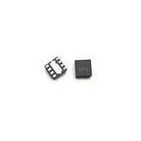
... Transmit/Receive switching application housed in QFN 2x2mm size package which is having good thermal resistance. The unique with 8 dies in parallel configuration results to low IL performance and low series resistance. The HSMP- 386J Power diode is built with match diode to ensure con- sistency in performance. Package Marking & Orientation ...

Page 2

Table 1. Absolute Maximum Ratings Symbol Parameter I Forward Current (1µs Pulse) per die F P Peak Inverse Voltage IV T Junction Temperature j T Storage Temperature stg θ Thermal Resistance Power Dissipation diss Notes: ...

Page 3

10.0 1.0 0.1 0.0 0.0 0.2 0.4 0 FORWARD VOLTAGE (V) F Figure 1. Forward Current vs. Forward Voltage 2.5 2.0 1.5 ...

Page 4

QFN 2x2 Package Dimension Pin 1 Dot By Marking 2.000±0.050 6Px 2.000±0.050 Top View 0.800±0.050 Exp.DAP 0.500 Bsc 1.600±0.050 Exp.DAP 0.250±0.050 0.250 Bottom View Note: 1. All dimensions in millimeters. 2. Dimensions are inclusive of plating. 3. Dimensions are exclusive ...

Page 5

... PCB Land Pattern B (top view) Note : 1. All dimensions in millimeters (mils). 2. For PCB land pattern B and stencil layout B, external trace is required to connect all cathode pads as one single pad. Ordering Information Part Number No. of Devices HSMP-386J-TR1G 3000 HSMP-386J-TR2G 10000 HSMP-386J-BLKG 100 5 1.00 ...

Page 6

Device Orientation REEL USER FEED DIRECTION COVER TAPE Tape Dimensions 10° Max A 0 DESCRIPTION CAVITY LENGTH WIDTH DEPTH PITCH BOTTOM HOLE DIAMETER PERFORATION DIAMETER PITCH POSITION CARRIER TAPE WIDTH THICKNESS COVER TAPE WIDTH TAPE ...

Related keywords