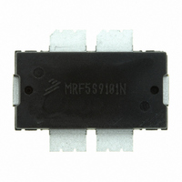
MRF5S9101NR1 Freescale Semiconductor, MRF5S9101NR1 Datasheet

MRF5S9101NR1
Specifications of MRF5S9101NR1
Available stocks
Related parts for MRF5S9101NR1
MRF5S9101NR1 Summary of contents
Page 1
... Freescale Semiconductor Technical Data Replaced by MRF5S9101NR1/NBR1. There are no form, fit or function changes with this part replacement. N suffix added to part number to indicate transition to lead - free terminations. RF Power Field Effect Transistors N - Channel Enhancement - Mode Lateral MOSFETs Designed for GSM and GSM EDGE base station applications with frequencies from 869 to 960 MHz ...
Page 2
... Vdc — 3.7 — Vdc — 0.21 0.3 Vdc — 7 — S — 70 — pF — 2.2 — 700 mA 960 MHz — % — 100 110 — W (continued) RF Device Data Freescale Semiconductor ...
Page 3
... Typical GSM EDGE Performances (In Freescale GSM EDGE Test Fixture, 50 οhm system 650 mA, 869 MHz<Frequency<894 MHz, 920 MHz<Frequency<960 MHz DQ Power Gain Drain Efficiency Error Vector Magnitude Spectral Regrowth at 400 kHz Offset Spectral Regrowth at 600 kHz Offset RF Device Data Freescale Semiconductor (continued) = 25°C unless otherwise noted) C Symbol G ps η D EVM ...
Page 4
... Microstrip (quarter wave length for bias purpose) Taconic TLX8 - 0300, 0.030″, ε = 2.55 r Part Number Manufacturer Murata ATC ATC ATC ATC ATC ATC ATC ATC Sprague RF Device Data Freescale Semiconductor RF OUTPUT ...
Page 5
... R2 C10 C19 Freescale has begun the transition of marking Printed Circuit Boards (PCBs) with the Freescale Semiconductor signature/logo. PCBs may have either Motorola or Freescale markings during the transition period. These changes will have no impact on form, fit or function of the current product. Figure 2. MRF5S9101MR1(MBR1) 900 MHz Test Circuit Component Layout ...
Page 6
... Watts CW out Vdc 940 MHz 100 1000 Figure 6. Power Gain versus Output Power −15 −30 −45 1000 1020 −8 −12 −16 −20 −24 1000 1020 100 120 140 160 180 P , OUTPUT POWER (WATTS) CW out RF Device Data Freescale Semiconductor 32 V 200 ...
Page 7
... SR 600 kHz 40 W Avg Avg Avg. − Avg. −83 900 910 920 930 940 950 f, FREQUENCY (MHz) Figure 10. Spectral Regrowth at 400 kHz and 600 kHz versus Frequency RF Device Data Freescale Semiconductor TYPICAL CHARACTERISTICS - 900 MHz 70 3 −30_C 25_C 85_C 2 1.5 20 ...
Page 8
... This above graph displays calculated MTTF in hours x ampere drain current. Life tests at elevated temperatures have correlated to better than ±10% of the theoretical prediction for metal failure. Divide 2 MTTF factor by I for MTTF in a particular application 85_C C −30_C 210 2 RF Device Data Freescale Semiconductor ...
Page 9
... C16, C22 6.8 pF 100B Chip Capacitors C18 5.6 pF 100B Chip Capacitor C19, C20 2.7 pF 100B Chip Capacitors C21 220 mF Electrolytic Capacitor, Axial R1 kW, 1/4 W Chip Resistors (1206 1/4 W Chip Resistor (1206) RF Device Data Freescale Semiconductor C7 Z14 R3 C16 DUT C22 C17 Z10 Z11 ...
Page 10
... C19 800 MHz Rev 2 Freescale has begun the transition of marking Printed Circuit Boards (PCBs) with the Freescale Semiconductor signature/logo. PCBs may have either Motorola or Freescale markings during the transition period. These changes will have no impact on form, fit or function of the current product. ...
Page 11
... FREQUENCY (MHz) Figure 18. Error Vector Magnitude versus Frequency RF Device Data Freescale Semiconductor TYPICAL CHARACTERISTICS - 800 MHz Vdc 700 mA DQ 830 840 850 860 870 880 890 900 910 920 930 f, FREQUENCY (MHz) out ps D ...
Page 12
... Figure 21. Spectral Regrowth at 400 kHz Vdc 650 880 MHz T = 25_C OUTPUT POWER (WATTS) AVG. out Figure 22. Spectral Regrowth at 600 kHz versus Output Power T = 25_C Vdc 650 880 MHz OUTPUT POWER (WATTS) AVG. out versus Output Power Device Data Freescale Semiconductor 80 90 ...
Page 13
... MHz f = 845 MHz Z load Figure 23. Series Equivalent Source and Load Impedance RF Device Data Freescale Semiconductor f = 845 MHz Z source f = 990 MHz = 5 Ω Vdc 700 mA 100 out source load MHz Ω Ω 845 4.29 - j2.23 1.15 - j0.04 865 3.94 - j1.24 1.05 - j0.10 890 2 ...
Page 14
... MRF5S9101MR1 MRF5S9101MBR1 14 NOTES RF Device Data Freescale Semiconductor ...
Page 15
... RF Device Data Freescale Semiconductor NOTES MRF5S9101MR1 MRF5S9101MBR1 15 ...
Page 16
... E5 .346 .350 8.79 8.89 F .025 BSC 0.64 BSC b1 .164 .170 4.17 4.32 c1 .007 .011 0.18 0.28 e .106 BSC 2.69 BSC aaa .004 0.10 STYLE 1: PIN 1. DRAIN 2. DRAIN 3. GATE 4. GATE 5. SOURCE RF Device Data Freescale Semiconductor ...
Page 17
... RF Device Data Freescale Semiconductor MRF5S9101MR1 MRF5S9101MBR1 17 ...
Page 18
... MRF5S9101MR1 MRF5S9101MBR1 18 RF Device Data Freescale Semiconductor ...
Page 19
... RF Device Data Freescale Semiconductor MRF5S9101MR1 MRF5S9101MBR1 19 ...
Page 20
... Freescale Semiconductor product could create a situation where personal injury or death may occur. Should Buyer ...


