NE5520379A-A CEL, NE5520379A-A Datasheet
NE5520379A-A
Specifications of NE5520379A-A


Related parts for NE5520379A-A


NE5520379A-A Summary of contents
Page 1
To our customers, Old Company Name in Catalogs and Other Documents st On April 1 , 2010, NEC Electronics Corporation merged with Renesas Technology Corporation, and Renesas Electronics Corporation took over all the business of both companies. Therefore, although the ...
Page 2
All information included in this document is current as of the date this document is issued. Such information, however, is subject to change without any prior notice. Before purchasing or using any Renesas Electronics products listed herein, please confirm ...
Page 3
... FOR GSM/DCS DUAL-BAND PHONE TRANSMISSION AMPLIFIERS DESCRIPTION The NE5520379A is an N-channel silicon power MOS FET specially designed as the transmission power amplifier for 3.2 V GSM 900 handsets. Dies are manufactured using our NEWMOS technology and housed in a surface mount package. This device can deliver 34.6 dBm output power with 68% power efficiency at 915 MHz under the 2.8 V supply voltage ...
Page 4
... C) A Ratings Unit 15.0 V 5.0 V 1 tot °C 125 ch −65 to +125 °C Test Conditions DS GS Duty Cycle ≤ 50%, T ≤ 1.8 GHz 3 Data Sheet PU10122EJ03V0DS NE5520379A MIN. TYP. MAX. Unit 2.8 3.2 6 2.5 3.5 V − 1.75 2 dBm ...
Page 5
... 2.5 V, Note add 785 MHz dBm 3 2.5 V, Note 785 MHz dBm, out 3 2.5 V, Note add Data Sheet PU10122EJ03V0DS NE5520379A MIN. TYP. MAX. Unit − − 100 nA − − 100 nA 1.0 1.35 2.0 V − − 2.5 S − − − °C/W 5 − ...
Page 6
... DRAIN EFFICIENCY, POWER ADDED EFFICIENCY vs. GATE TO SOURCE VOLTAGE 100 2 500 915 MHz dBm in 2 000 1 500 50 1 000 500 0 4.0 0 1.0 (V) Gate to Source Voltage V Data Sheet PU10122EJ03V0DS NE5520379A 2.0 2.5 3.0 (V) GS η d η add Input Power P (dBm) in η d η add 2.0 3 ...
Page 7
... Input Power P DRAIN EFFICIENCY, POWER ADDED EFFICIENCY vs. GATE TO SOURCE VOLTAGE 2 500 100 785 MHz dBm in 2 000 1 500 50 1 000 500 0 4.0 0 1.0 Gate to Source Voltage V Data Sheet PU10122EJ03V0DS NE5520379A η d η add (dBm) in η d η add (dBm) in η d η ...
Page 8
... MHz 2 000 1 500 50 1 000 500 DRAIN EFFICIENCY, POWER ADDED EFFICIENCY vs. INPUT POWER 100 2 500 150 mA Dset f = 460 MHz 2 000 1 500 50 1 000 500 Data Sheet PU10122EJ03V0DS NE5520379A η d η add Input Power P (dBm) in η d η add Input Power P (dBm) in ...
Page 9
... Microwave] → [Device Parameters] URL http://www.csd-nec.com/ LARGE SIGNAL IMPEDANCE ( (MHz) Z (Ω 785 TBD Note Z is the conjugate of optimum load impedance at given voltage, idling current, input power and frequency 3 600 mA dBm) Dset in Note (Ω) OL TBD Data Sheet PU10122EJ03V0DS NE5520379A 7 ...
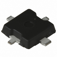
Page 10
... PACKAGE RECOMMENDED P.C.B. LAYOUT (UNIT: mm) Gate 8 (Bottom View) 1.5±0.2 Source Drain Gate 3.6±0.2 4.0 1.7 Source Stop up the hole with a rosin or something to avoid solder flow. Drain φ Through Hole: 0.2 × 33 0.5 0.5 6.1 Data Sheet PU10122EJ03V0DS NE5520379A Drain 0.8 MAX. ...
Page 11
... Data Sheet PU10122EJ03V0DS NE5520379A For soldering Condition Symbol IR260 VP215 WS260 HS350-P3 9 ...
Page 12
... NEC Corporation, NEC Compound Semiconductor Devices, Ltd. and also includes its majority-owned subsidiaries. (2) "NEC semiconductor products" means any semiconductor product developed or manufactured by or for NEC (as defined above). 10 Please check with an NEC sales representative for Data Sheet PU10122EJ03V0DS NE5520379A The M8E 00 0110 ...
Page 13
... TEL: +852-3107-7303 Taipei Branch Office TEL: +886-2-8712-0478 TEL: +82-2-558-2120 Korea Branch Office NEC Electronics (Europe) GmbH http://www.ee.nec.de/ TEL: +49-211-6503-01 FAX: +49-211-6503-487 California Eastern Laboratories, Inc. http://www.cel.com/ TEL: +1-408-988-3500 FAX: +1-408-988-0279 http://www.csd-nec.com/ FAX: +852-3107-7309 FAX: +886-2-2545-3859 FAX: +82-2-558-5209 NE5520379A 0306 ...