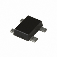
NE3509M04-A CEL, NE3509M04-A Datasheet

NE3509M04-A
Specifications of NE3509M04-A
Related parts for NE3509M04-A
NE3509M04-A Summary of contents
Page 1
... GPS antenna LNA • Low noise amplifier for microwave communication system ORDERING INFORMATION Part Number Order Number NE3509M04 NE3509M04-A NE3509M04-T2 NE3509M04-T2-A Remark To order evaluation samples, contact your nearby sales office. Part number for sample order: NE3509M04 ABSOLUTE MAXIMUM RATINGS (T Parameter ...
Page 2
... Unit − − − − 0 dBm in = +25°C, unless otherwise specified) A Test Conditions = − µ mA GHz (Non-RF GHz Data Sheet PG10608EJ01V0DS NE3509M04 MIN. TYP. MAX. Unit µ − 0 −0.25 −0.5 −0.75 V − − − 0.4 0.7 dB − 16 17.5 dB − − 11 dBm ...
Page 3
... Drain to Source Voltage V MINIMUM NOISE FIGURE, ASSOCIATED GAIN vs. DRAIN TO SOURCE VOLTAGE 20 2 2.0 GHz 1 1.6 14 1.4 12 1.2 10 1.0 8 0.8 6 0.6 4 0.4 2 0.2 0 0.0 40 1.0 1.5 Drain to Source Voltage V Data Sheet PG10608EJ01V0DS NE3509M04 –0.6 –0.4 –0 –0.1 V –0.2 V –0.3 V –0.4 V –0 ( ...
Page 4
... Drain to Source Voltage V DRAIN CURRENT 3, OIP = +25 dBm 3 IIP = +7.5 dBm ( ( 2.5 GHz (Non-RF) D –15 –10 – Input Power P (dBm tone) Data Sheet PG10608EJ01V0DS NE3509M04 min 2.0 2.5 3.0 3.5 ( ...
Page 5
... S-PARAMETERS S-parameters/Noise parameters are provided on our web site in a form (S2P) that enables direct import to a microwave circuit simulator without keyboard input. Click here to download S-parameters. [RF and Microwave] → [Device Parameters] URL http://www.ncsd.necel.com/ Data Sheet PG10608EJ01V0DS NE3509M04 5 ...
Page 6
... PACKAGE DIMENSIONS FLAT-LEAD 4-PIN THIN-TYPE SUPER MINIMOLD (M04) (UNIT: mm) 2.05±0.1 1.25±0.1 6 (Bottom View) PIN CONNECTIONS 1. Source 2. Drain 3. Source 4. Gate Data Sheet PG10608EJ01V0DS NE3509M04 (1.05) ...
Page 7
... MOUNTING PAD DIMENSIONS (REFERENCE ONLY) FLAT-LEAD 4-PIN THIN-TYPE SUPER MINIMOLD (M04) PACKAGE (UNIT: mm) 1.6 0.6 Data Sheet PG10608EJ01V0DS NE3509M04 7 ...
Page 8
... Caution Do not use different soldering methods together (except for partial heating). 8 Soldering Conditions : 260°C or below : 10 seconds or less : 60 seconds or less : 120±30 seconds : 3 times : 0.2%(Wt.) or below : 350°C or below : 3 seconds or less : 0.2%(Wt.) or below Data Sheet PG10608EJ01V0DS NE3509M04 For soldering Condition Symbol IR260 HS350 ...
Page 9
... CAS numbers and other limited information may not be available for release event shall CEL’s liability arising out of such information exceed the total purchase price of the CEL part(s) at issue sold by CEL to customer on an annual basis. ...


