BLF6G27-75,112 NXP Semiconductors, BLF6G27-75,112 Datasheet
BLF6G27-75,112
Specifications of BLF6G27-75,112


Related parts for BLF6G27-75,112


BLF6G27-75,112 Summary of contents
Page 1
... BLF6G27-75; BLF6G27LS-75 WiMAX power LDMOS transistor Rev. 01 — 22 October 2009 1. Product profile 1.1 General description 75 W LDMOS power transistor for base station applications at frequencies from 2500 MHz to 2700 MHz. Table 1. RF performance at T Mode of operation 1-carrier N-CDMA [1] Single carrier IS-95 with pilot, paging, sync and 6 traffic channels (Walsh codes 8 - 13). PAR = 9 ...
Page 2
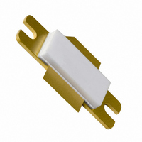
... Limiting values Table 4. In accordance with the Absolute Maximum Rating System (IEC 60134). Symbol stg T j BLF6G27-75_6G27LS-75_1 Product data sheet BLF6G27-75; BLF6G27LS-75 Pinning Description drain gate source drain gate source Ordering information Package Name Description - flanged LDMOST ceramic package; 2 mounting holes; 2 leads - earless fl ...
Page 3
... D ACPR 885k ACPR 1980k P L(M) [1] Measured within 30 kHz bandwidth. [2] Measured at 2.7 GHz and 3 dB compression of the CCDF at 0.01 % probability. BLF6G27-75_6G27LS-75_1 Product data sheet BLF6G27-75; BLF6G27LS-75 Thermal characteristics Parameter Conditions thermal resistance from T case junction to case (CW) L Characteristics Conditions drain-source breakdown ...
Page 4
... NXP Semiconductors 7.1 Ruggedness in class-AB operation The BLF6G27-75 and BLF6G27LS-75 are capable of withstanding a load mismatch corresponding to VSWR = through all phases under the following conditions 7.2 One-tone (dB) 18 (1) ( 600 mA ( 2500 MHz ( 2600 MHz ( 2700 MHz Fig 1. Power gain as a function of load power; ...
Page 5
... 600 mA ( 2500 MHz ( 2600 MHz ( 2700 MHz Fig 5. Adjacent channel power ratio (885 kHz function of load power; typical values BLF6G27-75_6G27LS-75_1 Product data sheet BLF6G27-75; BLF6G27LS-75 001aak976 (%) (W) L Fig 4. 001aak978 ACPR (dBc (W) L Fig 6. Rev. 01 — 22 October 2009 WiMAX power LDMOS transistor ...
Page 6
... 600 mA ( 2500 MHz ( 2600 MHz ( 2700 MHz Fig 9. Adjacent channel power ratio (5 MHz function of load power; typical values BLF6G27-75_6G27LS-75_1 Product data sheet BLF6G27-75; BLF6G27LS-75 001aak980 (%) (W) L Fig 8. 001aak982 ACPR (dBc (W) L Fig 10. Adjacent channel power ratio (10 MHz Rev. 01 — 22 October 2009 ...
Page 7
... 600 mA; carrier spacing = 10 MHz ( 2500 MHz ( 2600 MHz ( 2700 MHz Fig 13. Adjacent channel power ratio (5 MHz function of load power; typical values BLF6G27-75_6G27LS-75_1 Product data sheet BLF6G27-75; BLF6G27LS-75 001aak984 (%) (W) L Fig 12. Drain efficiency as a function of load power; 001aak986 ACPR (dBc (W) L Fig 14. Adjacent channel power ratio (10 MHz Rev. 01 — ...
Page 8
... Impedance information Table 8. Typical values per section unless otherwise specified. f GHz 2.5 2.6 2.7 Fig 15. Definition of transistor impedance 8.2 Test circuit C1 Fig 16. Component layout BLF6G27-75_6G27LS-75_1 Product data sheet BLF6G27-75; BLF6G27LS-75 Typical impedance Z S 5.3 j7.7 8.7 j8.7 12.2 + j0.4 gate ...
Page 9
... R1, R2 [1] American Technical Ceramics type 100A or capacitor of same quality. [2] American Technical Ceramics type 100B or capacitor of same quality. BLF6G27-75_6G27LS-75_1 Product data sheet BLF6G27-75; BLF6G27LS-75 List of components for component layout. Description ferrite bead multilayer ceramic chip capacitor multilayer ceramic chip capacitor multilayer ceramic chip capacitor ...
Page 10
... UNIT 12.83 4.72 0.15 20.02 mm 12.57 3.43 0.08 19.61 0.186 0.505 0.788 0.006 inches 0.135 0.495 0.772 0.003 OUTLINE VERSION IEC SOT502A Fig 17. Package outline SOT502A BLF6G27-75_6G27LS-75_1 Product data sheet BLF6G27-75; BLF6G27LS- scale 19.96 9.50 9.53 1.14 19.94 5.33 19.66 9.30 9 ...
Page 11
... DIMENSIONS (millimetre dimensions are derived from the original inch dimensions) c UNIT 12.83 4.72 0.15 20.02 mm 12.57 3.43 0.08 19.61 0.186 0.505 0.788 0.006 inches 0.135 0.495 0.772 0.003 OUTLINE VERSION IEC SOT502B Fig 18. Package outline SOT502B BLF6G27-75_6G27LS-75_1 Product data sheet BLF6G27-75; BLF6G27LS- scale 19.96 9.50 9.53 1.14 19.94 5.33 19.66 9 ...
Page 12
... PAR RF SMD VSWR W-CDMA WiMAX 11. Revision history Table 11. Revision history Document ID Release date BLF6G27-75_6G27LS-75_1 20091022 BLF6G27-75_6G27LS-75_1 Product data sheet BLF6G27-75; BLF6G27LS-75 Abbreviations Description Complementary Cumulative Distribution Function Continuous Wave Interim Standard 95 Laterally Diffused Metal-Oxide Semiconductor Laterally Diffused Metal-Oxide Semiconductor Transistor Narrowband Code Division Multiple Access ...
Page 13
... For more information, please visit: For sales office addresses, please send an email to: BLF6G27-75_6G27LS-75_1 Product data sheet BLF6G27-75; BLF6G27LS-75 [3] Definition This document contains data from the objective specification for product development. This document contains data from the preliminary specification. ...
Page 14
... Please be aware that important notices concerning this document and the product(s) described herein, have been included in section ‘Legal information’. © NXP B.V. 2009. For more information, please visit: http://www.nxp.com For sales office addresses, please send an email to: salesaddresses@nxp.com All rights reserved. Date of release: 22 October 2009 Document identifier: BLF6G27-75_6G27LS-75_1 ...