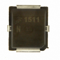
MRF1511NT1 Freescale Semiconductor, MRF1511NT1 Datasheet

MRF1511NT1
Specifications of MRF1511NT1
MRF1511NT1TR
Available stocks
Related parts for MRF1511NT1
MRF1511NT1 Summary of contents
Page 1
... BROADBAND RF POWER MOSFET CASE 466 - 03, STYLE 1 PLD - 1.5 PLASTIC Symbol Value V - 0.5, +40 DSS V ± 62 +150 stg T 150 J (2) Symbol Value R 2 θJC Package Peak Temperature 260 MRF1511NT1 Unit Vdc Vdc Adc W W/°C °C °C Unit °C/W Unit °C 1 ...
Page 2
... DS GS Functional Tests (In Freescale Test Fixture) Common - Source Amplifier Power Gain (V = 7.5 Vdc Watts 150 mA 175 MHz) DD out DQ Drain Efficiency (V = 7.5 Vdc Watts 150 mA 175 MHz) DD out DQ MRF1511NT1 2 = 25°C unless otherwise noted) Symbol I DSS I GSS V GS(th) V DS(on) C iss C oss C rss G ps η ...
Page 3
... Microstrip 1.057″ x 0.080″ Microstrip 0.120″ x 0.080″ Microstrip ® Glass Teflon , 31 mils, 2 oz. Copper 135 MHz 175 MHz 155 MHz OUTPUT POWER (WATTS) out Figure 3. Input Return Loss versus Output Power MRF1511NT1 RF OUTPUT 10 3 ...
Page 4
... MHz 8 135 MHz 175 MHz 200 400 600 I , BIASING CURRENT (mA) DQ Figure 6. Output Power versus Biasing Current 14 12 175 MHz SUPPLY VOLTAGE (VOLTS) DD Figure 8. Output Power versus Supply Voltage MRF1511NT1 7 Figure 5. Drain Efficiency versus Output Power 7 dBm in 40 800 1000 ...
Page 5
... Microstrip 0.490″ x 0.080″ Microstrip 0.872″ x 0.080″ Microstrip 0.206″ x 0.080″ Microstrip ® Glass Teflon , 31 mils, 2 oz. Copper MHz 66 MHz 77 MHz OUTPUT POWER (WATTS) out Figure 12. Input Return Loss versus Output Power MRF1511NT1 RF OUTPUT ...
Page 6
... MHz 66 MHz 200 400 600 I , BIASING CURRENT (mA) DQ Figure 15. Output Power versus Biasing Current MHz 8 66 MHz 88 MHz SUPPLY VOLTAGE (VOLTS) DD Figure 17. Output Power versus Supply Voltage MRF1511NT1 MHz 7 Figure 14. Drain Efficiency versus 7 25.7 dBm in 40 800 1000 0 Figure 16. Drain Efficiency versus ...
Page 7
... JUNCTION TEMPERATURE (°C) J This above graph displays calculated MTTF in hours x ampere drain current. Life tests at elevated temperatures have correlated to better than ±10% of the theoretical prediction for metal failure. Divide 2 MTTF factor by I for MTTF in a particular application. D 190 200 210 2 MRF1511NT1 7 ...
Page 8
... Figure 1 Complex conjugate of the load OL impedance at given output power, voltage, frequency, and η Note was chosen based on tradeoffs between gain, drain efficiency, and device stability. OL Figure 20. Series Equivalent Input and Output Impedance MRF1511NT1 175 MHz Ω Z 155 o 77 ...
Page 9
... S 22 ∠ φ ∠ φ 0.86 - 172 3 0.86 - 175 - 19 0.86 - 177 - 6 0.86 - 177 - 4 0.86 - 177 - 14 0.86 - 177 - 2 0.87 - 177 - 9 0.87 - 176 - 3 0.88 - 176 - 8 0.88 - 176 - 15 0.88 - 176 MRF1511NT1 9 ...
Page 10
... One critical figure of merit for a FET is its static resistance in the full - on condition. This on - resistance the linear region of the output characteristic and is speci- fied at a specific gate - source voltage and drain current. The MRF1511NT1 10 APPLICATIONS INFORMATION drain - source voltage under these conditions is termed V ...
Page 11
... Two - port stability analysis with this device’ parameters provides a useful tool for selection of loading or feedback circuitry to assure stable operation. See Free- scale Application Note AN215A, “RF Small - Signal Design Using Two - Port Parameters” for a discussion of two port network theory and stability. MRF1511NT1 11 ...
Page 12
... ZONE W 1 É É É É É É É É É É É É É É É É É É É É É É É É ZONE X VIEW MRF1511NT1 12 PACKAGE DIMENSIONS 0.35 (0.89 " NOTES: 1. INTERPRET DIMENSIONS AND TOLERANCES PER ASME Y14 ...
Page 13
... Modified data sheet to reflect MSL rating change from result of the standardization of packing process as described in Product and Process Change Notification number, PCN13516 • Added Electromigration MTTF Calculator availability to Product Documentation, Tools and Software Device Data Freescale Semiconductor REVISION HISTORY Description MRF1511NT1 13 ...
Page 14
... RoHS-compliant and/or Pb-free versions of Freescale products have the functionality and electrical characteristics of their non-RoHS-compliant and/or non-Pb-free counterparts. For further information, see http://www.freescale.com or contact your Freescale sales representative. For information on Freescale’s Environmental Products program http://www.freescale.com/epp. MRF1511NT1 Document Number: MRF1511N Rev. 8, 6/2009 14 Information in this document is provided solely to enable system and software implementers to use Freescale Semiconductor products ...


