MRF1570FNT1 Freescale Semiconductor, MRF1570FNT1 Datasheet
MRF1570FNT1
Specifications of MRF1570FNT1
Available stocks


Related parts for MRF1570FNT1


MRF1570FNT1 Summary of contents
Page 1
... RF POWER MOSFETs CASE 1366 - 05, STYLE 272 - 8 WRAP PLASTIC MRF1570NT1 CASE 1366A - 03, STYLE 272 - 8 PLASTIC MRF1570FNT1 Value Unit +0.5, +40 Vdc ± 20 Vdc 165 W 0.5 W/° +150 °C 200 °C (1) Value Unit 0.29 °C/W Class 1 (Minimum) M2 (Minimum) C2 (Minimum) Unit 260 °C MRF1570NT1 MRF1570FNT1 1 ...
Page 2
... RF Characteristics (In Freescale Test Fixture) Common - Source Amplifier Power Gain (V = 12.5 Vdc 800 mA) DD out DQ Drain Efficiency (V = 12.5 Vdc 800 mA) DD out DQ MRF1570NT1 MRF1570FNT1 2 = 25°C unless otherwise noted) Symbol f = 470 MHz f = 470 MHz Min Typ Max I — — 1 DSS V 1 — ...
Page 3
... Microstrip 0.27″ x 0.080″ Microstrip 0.25″ x 0.080″ Microstrip 0.29″ x 0.080″ Microstrip 0.14″ x 0.080″ Microstrip 0.32″ x 0.080″ Microstrip ® 31 mil Glass Teflon MRF1570NT1 MRF1570FNT1 V DD C30 RF OUTPUT C32 C31 ...
Page 4
... Figure 2. 135 - 175 MHz Broadband Test Circuit Component Layout TYPICAL CHARACTERISTICS, 135 - 175 MHz 100 80 135 MHz 60 175 MHz 40 150 MHz INPUT POWER (WATTS) in Figure 3. Output Power versus Input Power MRF1570NT1 MRF1570FNT1 4 C37 C38 C6 C10 C20 C22 C23 R4 C9 L10 L4 R2 ...
Page 5
... Vdc OUTPUT POWER (WATTS) out 155 MHz 175 MHz 135 MHz V = 12.5 Vdc dBm in 600 800 1000 1200 1400 I , BIASING CURRENT (mA) DQ 155 MHz 175 MHz 135 MHz dBm 800 SUPPLY VOLTAGE (VOLTS) DD MRF1570NT1 MRF1570FNT1 175 MHz 135 MHz 80 90 1600 15 5 ...
Page 6
... Chip Capacitors C25, C26 15 pF, 100 mil Chip Capacitors C27, C28 2.2 pF, 100 mil Chip Capacitors C29, C30 6.2 pF, 100 mil Chip Capacitors C31 1.0 pF, 100 mil Chip Capacitor Figure 11. 400 - 470 MHz Broadband Test Circuit Schematic MRF1570NT1 MRF1570FNT1 C10 C9 C37 ...
Page 7
... Figure 14. Input Return Loss versus Output Power V DD C33 B3 B4 GND C37 C34 C35 C36 C27 L3 L5 C29 L1 C31 C32 L2 C30 L6 L4 C28 C39 C40 C41 C42 B5 B6 C38 V = 12.5 Vdc DD 440 MHz 400 MHz 470 MHz OUTPUT POWER (WATTS) out MRF1570NT1 MRF1570FNT1 ...
Page 8
... I , BIASING CURRENT (mA) DQ Figure 17. Output Power versus Biasing Current 100 SUPPLY VOLTAGE (VOLTS) DD Figure 19. Output Power versus Supply Voltage MRF1570NT1 MRF1570FNT1 12.5 Vdc Figure 16. Drain Efficiency versus Output Power 100 80 470 MHz 440 MHz 400 MHz ...
Page 9
... Microstrip 0.14″ x 0.240″ Microstrip 0.15″ x 0.240″ Microstrip 0.18″ x 0.172″ Microstrip 1.23″ x 0.080″ Microstrip 0.12″ x 0.080″ Microstrip 0.40″ x 0.080″ Microstrip ® 31 mil Glass Teflon MRF1570NT1 MRF1570FNT1 RF 9 ...
Page 10
... Figure 22. 450 - 520 MHz Broadband Test Circuit Component Layout TYPICAL CHARACTERISTICS, 450 - 520 MHz 100 80 470 MHz 60 450 MHz 500 MHz 40 520 MHz INPUT POWER (WATTS) in Figure 23. Output Power versus Input Power MRF1570NT1 MRF1570FNT1 10 C33 C24 C6 L3 C20 C22 C21 C23 C7 C25 R2 C5 C14 ...
Page 11
... MHz dBm 800 Figure 30. Drain Efficiency versus Supply Voltage 520 MHz 500 MHz 450 MHz 470 MHz V = 12.5 Vdc OUTPUT POWER (WATTS) out V = 12.5 Vdc dBm in 800 1200 I , BIASING CURRENT (mA dBm 800 SUPPLY VOLTAGE (VOLTS) DD MRF1570NT1 MRF1570FNT1 80 90 1600 15 11 ...
Page 12
... This above graph displays calculated MTTF in hours x ampere drain current. Life tests at elevated temperatures have correlated to better than ±10% of the theoretical prediction for metal failure. Divide MTTF factor by I Figure 31. MTTF Factor versus Junction Temperature MRF1570NT1 MRF1570FNT1 12 TYPICAL CHARACTERISTICS 100 110 ...
Page 13
... Matching Under Test Network Ω 520 MHz f = 450 MHz 520 MHz out MHz Ω Ω 450 0.94 - j1.12 0.61 - j1.14 470 1.03 - j1.17 0.62 - j1.12 500 0.95 - j1.71 0.75 - j1.03 520 0.62 - j1.74 0.77 - j0.97 Output Matching Network MRF1570NT1 MRF1570FNT1 13 ...
Page 14
... One critical figure of merit for a FET is its static resistance in the full - on condition. This on - resistance the linear region of the output characteristic and is speci- fied at a specific gate - source voltage and drain current. The MRF1570NT1 MRF1570FNT1 14 APPLICATIONS INFORMATION drain - source voltage under these conditions is termed V ...
Page 15
... See Freescale Application Note AN215A, “RF Small - Signal Design Using Two - Port Parameters” for a discussion of two port network theory and stability. MRF1570NT1 MRF1570FNT1 15 ...
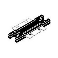
Page 16
... MRF1570NT1 MRF1570FNT1 16 PACKAGE DIMENSIONS RF Device Data Freescale Semiconductor ...
Page 17
... RF Device Data Freescale Semiconductor MRF1570NT1 MRF1570FNT1 17 ...
Page 18
... MRF1570NT1 MRF1570FNT1 18 RF Device Data Freescale Semiconductor ...
Page 19
... RF Device Data Freescale Semiconductor MRF1570NT1 MRF1570FNT1 19 ...
Page 20
... MRF1570NT1 MRF1570FNT1 20 RF Device Data Freescale Semiconductor ...
Page 21
... RF Device Data Freescale Semiconductor MRF1570NT1 MRF1570FNT1 21 ...
Page 22
... Product and Process Change Notification number, PCN13516 • Added AN3789, Clamping of High Power RF Transistors and RFICs in Over - Molded Plastic Packages to Product Documentation, Application Notes • Added Electromigration MTTF Calculator availability to Product Software MRF1570NT1 MRF1570FNT1 22 REVISION HISTORY Description RF Device Data ...
Page 23
... Freescale Semiconductor was negligent regarding the design or manufacture of the part. Freescalet and the Freescale logo are trademarks of Freescale Semiconductor, Inc. All other product or service names are the property of their respective owners. © Freescale Semiconductor, Inc. 2008-2009. All rights reserved. MRF1570NT1 MRF1570FNT1 23 ...