MRF282ZR1 Freescale Semiconductor, MRF282ZR1 Datasheet
MRF282ZR1
Specifications of MRF282ZR1
Available stocks


Related parts for MRF282ZR1

MRF282ZR1 Summary of contents
Page 1
... MRF282ZR1 Symbol Value Unit V - 0.5, +65 Vdc DSS V ± 20 Vdc 0.34 W/° +150 °C stg T 150 ° 200 °C J Symbol Value Unit R 4.2 °C/W θJC Min Typ Max Unit 65 — — Vdc — — 1.0 μAdc — — 1.0 μAdc MRF282SR1 MRF282ZR1 1 ...
Page 2
... W PEP mA, DD out 1930.0 MHz 1930.1 MHz) Common - Source Power Gain ( Vdc CW mA 2000.0 MHz) DD out DQ Drain Efficiency ( Vdc CW mA 2000.0 MHz) DD out DQ MRF282SR1 MRF282ZR1 2 (continued) = 25°C unless otherwise noted) C Symbol V GS(th) V DS(on) V GS(q) C iss C oss C rss G ps η IMD ...
Page 3
... Microstrip 0.452″ ± 0.085″ x 0.080″ Microstrip 0.910″ ± 0.085″ x 0.080″ Microstrip ® 0.030″ Glass Teflon , 2 oz Copper, 3″ x 5″ Dimensions, Arlon GX0300 - 55 - 22, ε = 2.55 r Description MRF282SR1 MRF282ZR1 C18 RF OUTPUT 3 ...
Page 4
... Freescale has begun the transition of marking Printed Circuit Boards (PCBs) with the Freescale Semiconductor signature/logo. PCBs may have either Motorola or Freescale markings during the transition period. These changes will have no impact on form, fit or function of the current product. Figure 2. 1930 - 2000 MHz Broadband Test Circuit Component Layout MRF282SR1 MRF282ZR1 4 C13 C7 ...
Page 5
... W Fixed Film Chip Resistors, Garrett Instruments #RM73B2B120JT 0.08″ x 0.13″ Resistors, Garrett Instruments #RM73B2B120JT Beryllium Copper 0.010″ x 0.110″ x 0.210″ C10 C13 C16 Z10 Z11 C15 C17 ® Copper, 3″ x 5″ Dimensions, Arlon GX0300 - 55 - 22, ε = 2.55 r MRF282SR1 MRF282ZR1 OUTPUT 5 ...
Page 6
... C1, C20 C2 C3, C10, C15 C4, C16 C5 C6, C7, C9, C14, C17 C8, C13 C11, C12 C18 C19 R4, R6 R8, R9, R10 Input/Output MRF282SR1 MRF282ZR1 DUT Z3 Z4 C11 C7 C10 Raw Board Material Ferrite Beads, Ferroxcube #56 - 590 - 470 μ Electrolytic Capacitors, Mallory #SME63V471M12X25L 0.01 μF Chip Capacitor, ATC #100B103JCA50X 0.6 - 4.5 pF Variable Capacitors, Johanson #27271SL 0.02 μ ...
Page 7
... Z = Complex conjugate of source impedance Complex conjugate of the optimum load OL impedance at given output power, voltage, IMD, bias current and frequency. Input Device Matching Under Test Network 1800 MHz * Output Matching Network MRF282SR1 MRF282ZR1 7 ...
Page 8
... MRF282SR1 MRF282ZR1 8 NOTES RF Device Data Freescale Semiconductor ...
Page 9
... RF Device Data Freescale Semiconductor NOTES MRF282SR1 MRF282ZR1 9 ...
Page 10
... MRF282SR1 MRF282ZR1 10 NOTES RF Device Data Freescale Semiconductor ...
Page 11
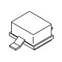
... Z −−− R .020 −−− bbb .010 REF 0.254 REF ccc .015 REF 0.381 REF STYLE 1: PIN 1. DRAIN 2. GATE 3. SOURCE MRF282SR1 MRF282ZR1 MAX 4.83 3.81 2.946 1.346 0.254 0.152 0.787 2.794 5.156 4.648 3.886 4.14 0.508 MAX 4 ...
Page 12
... P.O. Box 5405 Denver, Colorado 80217 1 - 800 - 441 - 2447 or 303 - 675 - 2140 Fax: 303 - 675 - 2150 LDCForFreescaleSemiconductor@hibbertgroup.com MRF282SR1 MRF282ZR1 Document Number: MRF282 Rev. 15, 5/2006 12 Information in this document is provided solely to enable system and software implementers to use Freescale Semiconductor products. There are no express or implied copyright licenses granted hereunder to design or fabricate any integrated circuits or integrated circuits based on the information in this document ...