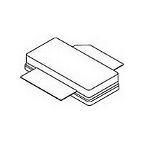
MRF7S21080HSR3 Freescale Semiconductor, MRF7S21080HSR3 Datasheet

MRF7S21080HSR3
Specifications of MRF7S21080HSR3
Available stocks
Related parts for MRF7S21080HSR3
MRF7S21080HSR3 Summary of contents
Page 1
... MHz AVG CASE 465- 06, STYLE 1 MRF7S21080HR3 CASE 465A - 06, STYLE 1 MRF7S21080HSR3 Symbol V DSS stg Symbol R θJC MRF7S21080HR3 MRF7S21080HSR3 Rev. 0, 11/2007 SINGLE W - CDMA LATERAL N - CHANNEL RF POWER MOSFETs NI - 780 NI - 780S Value Unit - 0.5, +65 Vdc - 6.0, +10 Vdc 32, +0 Vdc - 65 to +150 °C 150 °C 225 °C ...
Page 2
... Output Peak - to - Average Ratio @ 0.01% Probability on CCDF Adjacent Channel Power Ratio Input Return Loss Parameter measured on Freescale Test Fixture, due to resistive divider network on the board. Refer to Test Circuit GG GS(Q) schematic. 2. Part internally matched both on input and output. MRF7S21080HR3 MRF7S21080HSR3 2 = 25°C unless otherwise noted) C Symbol I DSS I DSS I ...
Page 3
... Min Typ Max = 800 mA, 2110 - 2170 MHz Bandwidth — 10 — — 0.12 — — 22.3 — — 6.21 — — 151.6 — — 0.009 — — 0.008 — MRF7S21080HR3 MRF7S21080HSR3 Unit MHz dB ° ns ° dB/°C dBm/°C 3 ...
Page 4
... Chip Capacitor C5, C12, C13, C14, C15 10 μ Chip Capacitors C6 1.5 pF Chip Capacitor C7, C8, C17 0.2 pF Chip Capacitors C16 220 μ Electrolytic Capacitor, Radial R1 KΩ, 1/4 W Chip Resistors R3 10 Ω, 1/4 W Chip Resistor MRF7S21080HR3 MRF7S21080HSR3 4 Z15 C10 C12 Z14 DUT ...
Page 5
... C17 C2 Figure 2. MRF7S21080HR3(HSR3) Test Circuit Component Layout RF Device Data Freescale Semiconductor C4 C12 C3 C10 R3 C11 C14 MRF7S21080H V DD C13 C16 C15 Rev. 1 MRF7S21080HR3 MRF7S21080HSR3 5 ...
Page 6
... Vdc 2135 MHz 2145 MHz DD Two−Tone Measurements, 10 MHz Tone Spacing OUTPUT POWER (WATTS) PEP out Figure 5. Two - Tone Power Gain versus Output Power MRF7S21080HR3 MRF7S21080HSR3 6 TYPICAL CHARACTERISTICS η Vdc (Avg.), I = 800 mA DD out DQ Single−Carrier W−CDMA, 3.84 MHz Channel Bandwidth Input Signal PAR = 7 ...
Page 7
... IM3−U IM5−U IM5−L IM7−U IM7−L 10 TWO−TONE SPACING (MHz) versus Tone Spacing 70 Ideal Actual −30_C T = −30_C C 25_C 85_C 85_C Vdc 800 2140 MHz 10 100 P , OUTPUT POWER (WATTS) CW out versus CW Output Power MRF7S21080HR3 MRF7S21080HSR3 100 70 60 25_C 200 7 ...
Page 8
... W−CDMA. ACPR Measured in 3.84 MHz Channel Bandwidth @ "5 MHz Offset. 0.001 Input Signal PAR = 7 0.01% Probability on CCDF 0.0001 PEAK−TO−AVERAGE (dB) Figure 14. CCDF W - CDMA 3GPP, Test Model 1, 64 DPCH, 50% Clipping, Single - Carrier Test Signal MRF7S21080HR3 MRF7S21080HSR3 8 TYPICAL CHARACTERISTICS 800 2140 MHz ...
Page 9
... Z = Test circuit impedance as measured from source gate to ground Test circuit impedance as measured load from drain to ground. Input Device Under Matching Test Network Z Z source load load W Output Matching Network MRF7S21080HR3 MRF7S21080HSR3 9 ...
Page 10
... (INSULATOR) bbb M N (LID) ccc (FLANGE (FLANGE (LID (FLANGE) D bbb (LID) ccc M M (INSULATOR) bbb SEATING T PLANE A A (FLANGE) MRF7S21080HR3 MRF7S21080HSR3 10 PACKAGE DIMENSIONS Q bbb (LID ccc (INSULATOR) aaa SEATING PLANE CASE 465 - 06 ISSUE 780 MRF7S21080HR3 Z R (LID ccc (INSULATOR) aaa ...
Page 11
... AN1955: Thermal Measurement Methodology of RF Power Amplifiers Engineering Bulletins • EB212: Using Data Sheet Impedances for RF LDMOS Devices The following table summarizes revisions to this document. Revision Date 0 Nov. 2007 • Initial Release of Data Sheet RF Device Data Freescale Semiconductor PRODUCT DOCUMENTATION REVISION HISTORY Description MRF7S21080HR3 MRF7S21080HSR3 11 ...
Page 12
... P.O. Box 5405 Denver, Colorado 80217 1 - 800 - 441 - 2447 or 303 - 675 - 2140 Fax: 303 - 675 - 2150 LDCForFreescaleSemiconductor@hibbertgroup.com MRF7S21080HR3 MRF7S21080HSR3 Document Number: MRF7S21080H Rev. 0, 11/2007 12 Information in this document is provided solely to enable system and software implementers to use Freescale Semiconductor products. There are no express or implied copyright licenses granted hereunder to design or fabricate any integrated circuits or integrated circuits based on the information in this document ...


