NESG2031M05-A CEL, NESG2031M05-A Datasheet - Page 2
NESG2031M05-A
Manufacturer Part Number
NESG2031M05-A
Description
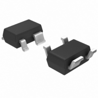
TRANS NPN 2GHZ SOT-343
Manufacturer
CEL
Datasheet
1.NESG2031M05-T1-A.pdf
(13 pages)
Specifications of NESG2031M05-A
Transistor Type
NPN
Voltage - Collector Emitter Breakdown (max)
5V
Frequency - Transition
25GHz
Noise Figure (db Typ @ F)
0.8dB ~ 1.3dB @ 2GHz ~ 5.2GHz
Gain
10dB ~ 17dB
Power - Max
175mW
Dc Current Gain (hfe) (min) @ Ic, Vce
130 @ 5mA, 2V
Current - Collector (ic) (max)
35mA
Mounting Type
Surface Mount
Package / Case
SC-70-4, SC-82-4, SOT-323-4, SOT-343
Continuous Collector Current
35 mA
Emitter- Base Voltage Vebo
1.5 V
Mounting Style
SMD/SMT
Power Dissipation
175 mW
Lead Free Status / RoHS Status
Lead free / RoHS Compliant
Lead Free Status / RoHS Status
Lead free / RoHS Compliant, Lead free / RoHS Compliant
Available stocks
Company
Part Number
Manufacturer
Quantity
Price
Company:

Part Number:
NESG2031M05-A
Manufacturer:
CEL
Quantity:
135


ABSOLUTE MAXIMUM RATINGS
Note:
1. Operation in excess of any one of these parameters may result
2. Mounted on 1.08 cm
TYPICAL PERFORMANCE CURVES
SYMBOLS
in permanent damage.
V
V
V
T
P
CBO
CEO
EBO
T
STG
I
C
T
J
2
0.0001
0.001
0.01
100
250
200
150
100
0.1
175
50
10
1
0
0.4
Collector to Base Voltage
Collector to Emitter Voltage
Emitter to Base Voltage
Collector Current
Total Power Dissipation
Junction Temperature
Storage Temperature
TOTAL POWER DISSIPATION vs.
V
BASE TO EMITTER VOLTAGE
CE
Base to Emitter Voltage, V
PARAMETERS
COLLECTOR CURRENT vs.
Ambient Temperature, T
0.5
25
AMBIENT TEMPERATURE
= 1 V
2
x 1.0 mm (t) glass epoxy PCB.
0.6
50
Mounted on Glass Epoxy PCB
(1.08 cm
0.7
75
2
× 1.0 mm (t) )
100
0.8
1
UNITS
A
(T
mW
BE
mA
(°C)
°C
°C
V
V
V
A
125
0.9
(T
(V)
= 25°C)
A
= 25ºC)
150
1.0
-65 to +150
RATINGS
13.0
175
150
5.0
1.5
35
THERMAL RESISTANCE
ORDERING INFORMATION
SYMBOLS
NESG2031M05-T1
NESG2031M05-T1-A 3 kpcs/reel • Pb Free
PART NUMBER
R
th j-c
0.0001
0.001
0.01
100
0.3
0.2
0.1
0.1
10
Junction to Case Resistance
0
1
0.4
REVERSE TRANSFER CAPACITANCE
vs. COLLECTOR TO BASE VOLTAGE
V
Collector to Base Voltage, V
CE
PARAMETERS
BASE TO EMITTER VOLTAGE
Base to Emitter Voltage, V
0.5
COLLECTOR CURRENT vs.
= 2 V
2
QUANTITY
3 kpcs/reel • Pin 3 (Collector), Pin 4
0.6
4
0.7
• 8 mm wide embossed
• Pin 3 (Collector), Pin 4
• 8 mm wide embossed
(Emitter) face the perforation
taping
(Emitter) face the perforation
taping
6
0.8
SUPPLY FORM
UNITS
NESG2031M05
°C/W
f = 1 MHz
BE
CB
8
0.9
(V)
(V)
10
1.0
RATINGS
TBD
Related parts for NESG2031M05-A
Image
Part Number
Description
Manufacturer
Datasheet
Request
R

Part Number:
Description:
Dantona CEL-V325-HC Cell Phone Battery Fits Motorola Q & BT-50
Manufacturer:
DANTONA INDUSTRIES
Part Number:
Description:
FRS RADIO BATTERIES 3.6 VOLTS / 1600 MAH
Manufacturer:
DANTONA INDUSTRIES
Part Number:
Description:
LITHIUM ION 900MA FOR USE WITH NOKIA 3360 CELL PHONE
Manufacturer:
DANTONA INDUSTRIES
Part Number:
Description:
CELL PHONE BATTERY FOR MOTOROLA V3 CELLULAR PHONE
Manufacturer:
DANTONA INDUSTRIES

Part Number:
Description:
Samsung SCH-A990 Li-Ion Replacement Cell Phone Battery
Manufacturer:
SAMSUNG
Part Number:
Description:
4.8V, 1300MAH, NIMH, FOR MOTOROLA & NEXTEL 2-WAY RADIO
Manufacturer:
DANTONA INDUSTRIES

Part Number:
Description:
Transistor Output Optocouplers DISC BY CEL 6/00 SO-6 PHOTOCOUPLER
Manufacturer:
CEL
Datasheet:
Part Number:
Description:
Transistor Output Optocouplers DISC BY CEL 8/00 DIP-6 PHOTO COUPLER
Manufacturer:
CEL
Datasheet:
Part Number:
Description:
Transistor Output Optocouplers DISC BY CEL 11/00 DIP-6 PHOTO COUPLER
Manufacturer:
CEL
Datasheet:
Part Number:
Description:
Transistor Output Optocouplers DISC BY CEL 6/00 DIP-6 PHOTO COUPLER
Manufacturer:
CEL
Datasheet:
Part Number:
Description:
Transistor Output Optocouplers DISC BY CEL 5/00 DIP-6 PHOTO COUPLER
Manufacturer:
CEL
Datasheet: