UPA814T-T1-A CEL, UPA814T-T1-A Datasheet

TRANSISTOR NPN FT=9GHZ SOT-36

UPA814T-T1-A

Manufacturer Part Number
UPA814T-T1-A
Description
TRANSISTOR NPN FT=9GHZ SOT-36
Manufacturer
CEL
Datasheet

Specifications of UPA814T-T1-A

Transistor Type
2 NPN (Dual)
Voltage - Collector Emitter Breakdown (max)
6V
Frequency - Transition
9GHz
Noise Figure (db Typ @ F)
1.5dB @ 2GHz
Power - Max
200mW
Dc Current Gain (hfe) (min) @ Ic, Vce
80 @ 3mA, 1V
Current - Collector (ic) (max)
100mA
Mounting Type
Surface Mount
Package / Case
SC-70-6, SC-88, SOT-363
Dc Collector/base Gain Hfe Min
80
Dc Current Gain Hfe Max
160
Mounting Style
SMD/SMT
Configuration
Single
Transistor Polarity
NPN
Emitter- Base Voltage Vebo
2 V
Continuous Collector Current
0.1 A
Power Dissipation
0.11 W
Lead Free Status / RoHS Status
Lead free / RoHS Compliant
Gain
-
Lead Free Status / RoHS Status
Lead free / RoHS Compliant, Lead free / RoHS Compliant
FEATURES
ELECTRICAL CHARACTERISTICS
• SMALL PACKAGE STYLE:
• LOW NOISE FIGURE:
• HIGH GAIN BANDWIDTH: f
• HIGH COLLECTOR CURRENT: 100 mA
NEC's UPA814T is two NPN high frequency silicon epitaxial
transistors encapsulated in an ultra small 6 pin SMT package.
Each transistor is independently mounted and easily config-
ured for either dual transistor or cascode operation. The high
f
various hand-held wireless applications.
DESCRIPTION
Notes: 1. Pulsed measurement, pulse width ≤ 350 µs, duty cycle ≤ 2 %.
ABSOLUTE MAXIMUM RATINGS
Note: 1.Operation in excess of any one of these parameters may
T
SYMBOLS
h
, low voltage bias and small size make this device suited for
SYMBOLS
FE1
|S
2 NE688 Die in a 2 mm x 1.25 mm package
NF = 1.5 dB TYP at 2 GHz
Cre
I
I
h
V
V
V
T
CBO
EBO
NF
21E
FE 1
f
P
/h
CBO
CEO
T
T
EBO
I
STG
C
2. The emitter terminal should be connected to the ground terminal of the 3 terminal capacitance bridge.
For Tape and Reel version use part number UPA814T-T1, 3K per reel.
T
J
2
FE2
|
2
result in permanent damage.
Collector Cutoff Current at V
Emitter Cutoff Current at V
Forward Current Gain at V
Gain Bandwidth at V
Feedback Capacitance at V
Insertion Power Gain at V
Noise Figure at V
h
Collector to Base Voltage
Collector to Emitter Voltage
Emitter to Base Voltage
Collector Current
Total Power Dissipation
Junction Temperature
Storage Temperature
FE
Ratio:
PARAMETERS
PARAMETERS AND CONDITIONS
1 Die
2 Die
h
h
FE1
FE2
PACKAGE OUTLINE
= Smaller Value of Q
= Larger Value of Q
CE
PART NUMBER
= 3 V, I
T
CE
= 9 GHz
= 3 V, I
CE
EB
CE
CB
C
CB
= 3 V, I
= 7 mA, f = 2 GHz
FREQUENCY TRANSISTOR
= 1 V, I
= 1 V, I
UNITS
= 1 V, I
C
mW
mW
= 5V, I
mA
°C
°C
V
V
V
= 20 mA, f = 2 GHz
1
C
C
C
1
or Q
=20 mA, f = 2 GHz
, or Q
1
E
E
= 0
= 3 mA
= 0
= 0, f = 1 MHz
(T
-65 to +150
(T
RATINGS
2
A
A
2
= 25°C)
100
110
200
150
= 25°C)
9
6
2
NPN SILICON HIGH
UNITS
GHz
µA
µA
dB
dB
pF
PIN OUT
1. Collector Transistor 1
2. Base Transistor 2
3. Collector Transistor 2
4. Emitter Transistor 2
5. Emitter Transistor 1
6. Base Transistor 1
Note:
Pin 3 is identified with a circle on the bottom of the package.
OUTLINE DIMENSIONS
2.0 ± 0.2
0.9 ± 0.1
1.3
California Eastern Laboratories
0.7
MIN
0.85
0.65
80
PACKAGE OUTLINE S06
2
3
1
2.1 ± 0.1
1.25 ± 0.1
0 ~ 0.1
UPA814T
TYP
0.75
S06
110
9.0
6.5
1.5
(Units in mm)
UPA814T
6
5
4
0.2 (All Leads)
0.15
MAX
0.85
+0.10
- 0.05
160
0.1
0.1

Related parts for UPA814T-T1-A

UPA814T-T1-A Summary of contents

Page 1

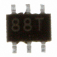
... FE2 Notes: 1. Pulsed measurement, pulse width ≤ 350 µs, duty cycle ≤ The emitter terminal should be connected to the ground terminal of the 3 terminal capacitance bridge. For Tape and Reel version use part number UPA814T-T1, 3K per reel. NPN SILICON HIGH FREQUENCY TRANSISTOR OUTLINE DIMENSIONS 2.0 ± ...

Page 2

... UPA814T TYPICAL PERFORMANCE CURVES TOTAL POWER DISSIPATION vs. AMBIENT TEMPERATURE 200 100 0 50 100 Ambient Temperature, T COLLECTOR CURRENT vs. COLLECTOR TO EMITTER VOLTAGE Collector to Emitter Voltage, V GAIN BANDWIDTH PRODUCT vs. COLLECTOR CURRENT GHz Collector Current 25°C) A Free Air 150 (°C) A 200 µA 180 µA 160 µA 140 µ ...

Page 3

... Frequency, f (GHz) ORDERING INFORMATION PART NUMBER QUANTITY UPA814T-T1-A 3000 Life Support Applications These NEC products are not intended for use in life support devices, appliances, or systems where the malfunction of these products can reasonably be expected to result in personal injury. The customers of CEL using or selling these products for use in such applications their own risk and agree to fully indemnify CEL for all damages resulting from such improper use or sale ...

Page 4

... CAS numbers and other limited information may not be available for release event shall CEL’s liability arising out of such information exceed the total purchase price of the CEL part(s) at issue sold by CEL to customer on an annual basis. ...

Related keywords