ST230S12P0V Vishay, ST230S12P0V Datasheet - Page 2
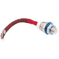
ST230S12P0V
Manufacturer Part Number
ST230S12P0V
Description
SCR PHASE CONT 1200V 230A TO-93
Manufacturer
Vishay
Specifications of ST230S12P0V
Scr Type
Standard Recovery
Voltage - Off State
1200V
Voltage - Gate Trigger (vgt) (max)
3V
Voltage - On State (vtm) (max)
1.55V
Current - On State (it (av)) (max)
230A
Current - On State (it (rms)) (max)
360A
Current - Gate Trigger (igt) (max)
150mA
Current - Hold (ih) (max)
600mA
Current - Off State (max)
30mA
Current - Non Rep. Surge 50, 60hz (itsm)
5700A, 5970A
Operating Temperature
-40°C ~ 125°C
Mounting Type
Chassis Mount
Package / Case
TO-209AB, TO-93
Current - On State (it (rms) (max)
360A
Breakover Current Ibo Max
5970 A
Rated Repetitive Off-state Voltage Vdrm
1200 V
Off-state Leakage Current @ Vdrm Idrm
30 mA
Forward Voltage Drop
1.55 V
Gate Trigger Voltage (vgt)
3 V
Maximum Gate Peak Inverse Voltage
5 V
Gate Trigger Current (igt)
150 mA
Holding Current (ih Max)
600 mA
Mounting Style
Stud
Peak Repetitive Off-state Voltage, Vdrm
1.2kV
Gate Trigger Current Max, Igt
150mA
Current It Av
230A
On State Rms Current It(rms)
360A
Peak Non Rep Surge Current Itsm 50hz
5.7kA
Lead Free Status / RoHS Status
Contains lead / RoHS non-compliant
Other names
*ST230S12P0V
VS-ST230S12P0V
VS-ST230S12P0V
VSST230S12P0V
VSST230S12P0V
VS-ST230S12P0V
VS-ST230S12P0V
VSST230S12P0V
VSST230S12P0V


ST230SPbF Series
Vishay High Power Products
www.vishay.com
2
ABSOLUTE MAXIMUM RATINGS
PARAMETER
Maximum average on-state current
at case temperature
Maximum RMS on-state current
Maximum peak, one-cycle
non-repetitive surge current
Maximum I
Maximum I
Low level value of threshold voltage
High level value of threshold voltage
Low level value of on-state slope resistance
High level value of on-state slope resistance
Maximum on-state voltage
Maximum holding current
Maximum (typical) latching current
SWITCHING
PARAMETER
Maximum non-repetitive rate of rise
of turned-on current
Typical delay time
Typical turn-off time
BLOCKING
PARAMETER
Maximum critical rate of rise
of off-state voltage
Maximum peak reverse and
off-state leakage current
2
2
t for fusing
√t for fusing
For technical questions, contact: ind-modules@vishay.com
SYMBOL
SYMBOL
SYMBOL
V
V
I
T(RMS)
dV/dt
I
I
dI/dt
I
I
T(TO)1
T(TO)2
V
RRM
T(AV)
I
DRM
TSM
I
2
r
r
t
t
I
I
2
TM
t1
t2
H
d
q
√t
L
t
Phase Control Thyristors
,
(Stud Version), 230 A
Gate drive 20 V, 20 Ω, t
T
Gate current 1 A, dI
V
I
V
T
T
180° conduction, half sine wave
DC at 78 °C case temperature
t = 10 ms
t = 8.3 ms
t = 10 ms
t = 8.3 ms
t = 10 ms
t = 8.3 ms
t = 10 ms
t = 8.3 ms
t = 0.1 to 10 ms, no voltage reapplied
(16.7 % x π x I
(I > π x I
(16.7 % x π x I
(I > π x I
I
T
TM
pk
J
J
d
R
J
J
= T
= 0.67 % V
= T
= T
= 25 °C, anode supply 12 V resistive load
= 720 A, T
= 50 V, dV/dt = 20 V/µs, gate 0 V 100 Ω, t
= 300 A, T
J
J
J
maximum linear to 80 % rated V
maximum, anode voltage ≤ 80 % V
maximum, rated V
T(AV)
T(AV)
), T
), T
J
DRM
No voltage
reapplied
100 % V
reapplied
No voltage
reapplied
100 % V
reapplied
J
T(AV)
T(AV)
= T
= T
J
J
TEST CONDITIONS
TEST CONDITIONS
TEST CONDITIONS
= T
= T
, T
J
J
< I < π x I
< I < π x I
maximum, t
g
maximum, dI/dt = 20 A/µs,
/dt = 1 A/µs
J
J
J
= 25 °C
maximum
maximum
RRM
RRM
r
≤ 1 µs
DRM
T(AV)
T(AV)
Sinusoidal half wave,
initial T
/V
p
RRM
= 10 ms sine pulse
), T
), T
applied
J
J
J
= T
= T
= T
DRM
J
J
J
DRM
maximum
maximum
maximum
p
= 500 µs
Document Number: 94399
1000 (300)
VALUES
VALUES
VALUES
Revision: 11-Aug-08
1000
5700
5970
4800
5000
1630
0.92
0.98
0.88
0.81
1.55
500
230
360
163
148
115
105
600
100
1.0
30
85
UNITS
UNITS
UNITS
kA
kA
V/µs
A/µs
mΩ
mA
mA
°C
µs
A
A
V
V
2
2
√s
s
Related parts for ST230S12P0V
Image
Part Number
Description
Manufacturer
Datasheet
Request
R

Part Number:
Description:
357-036-542-201 CARDEDGE 36POS DL .156 BLK LOPRO
Manufacturer:
Vishay
Datasheet:
Part Number:
Description:
357-036-542-201 CARDEDGE 36POS DL .156 BLK LOPRO
Manufacturer:
Vishay
Datasheet:
Part Number:
Description:
357-036-542-201 CARDEDGE 36POS DL .156 BLK LOPRO
Manufacturer:
Vishay
Datasheet:
Part Number:
Description:
357-036-542-201 CARDEDGE 36POS DL .156 BLK LOPRO
Manufacturer:
Vishay
Datasheet:
Part Number:
Description:
357-036-542-201 CARDEDGE 36POS DL .156 BLK LOPRO
Manufacturer:
Vishay
Datasheet:
Part Number:
Description:
357-036-542-201 CARDEDGE 36POS DL .156 BLK LOPRO
Manufacturer:
Vishay
Datasheet:
Part Number:
Description:
357-036-542-201 CARDEDGE 36POS DL .156 BLK LOPRO
Manufacturer:
Vishay
Datasheet:
Part Number:
Description:
357-036-542-201 CARDEDGE 36POS DL .156 BLK LOPRO
Manufacturer:
Vishay
Datasheet:
Part Number:
Description:
357-036-542-201 CARDEDGE 36POS DL .156 BLK LOPRO
Manufacturer:
Vishay
Datasheet:
Part Number:
Description:
357-036-542-201 CARDEDGE 36POS DL .156 BLK LOPRO
Manufacturer:
Vishay
Datasheet:
Part Number:
Description:
357-036-542-201 CARDEDGE 36POS DL .156 BLK LOPRO
Manufacturer:
Vishay
Datasheet:
Part Number:
Description:
357-036-542-201 CARDEDGE 36POS DL .156 BLK LOPRO
Manufacturer:
Vishay
Datasheet:
Part Number:
Description:
357-036-542-201 CARDEDGE 36POS DL .156 BLK LOPRO
Manufacturer:
Vishay
Datasheet:
Part Number:
Description:
357-036-542-201 CARDEDGE 36POS DL .156 BLK LOPRO
Manufacturer:
Vishay
Datasheet:
Part Number:
Description:
357-036-542-201 CARDEDGE 36POS DL .156 BLK LOPRO
Manufacturer:
Vishay
Datasheet: