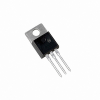
C122F1G ON Semiconductor, C122F1G Datasheet - Page 3

C122F1G
Manufacturer Part Number
C122F1G
Description
THYRISTOR SCR 8A 50V TO-220AB
Manufacturer
ON Semiconductor
Datasheet
1.C122F1G.pdf
(4 pages)
Specifications of C122F1G
Scr Type
Standard Recovery
Voltage - Off State
50V
Voltage - Gate Trigger (vgt) (max)
1.5V
Voltage - On State (vtm) (max)
1.83V
Current - On State (it (rms)) (max)
8A
Current - Gate Trigger (igt) (max)
25mA
Current - Hold (ih) (max)
30mA
Current - Off State (max)
10µA
Current - Non Rep. Surge 50, 60hz (itsm)
90A @ 60Hz
Operating Temperature
-40°C ~ 125°C
Mounting Type
Through Hole
Package / Case
TO-220-3 (Straight Leads)
Current - On State (it (rms) (max)
8A
Breakover Current Ibo Max
90 A
Rated Repetitive Off-state Voltage Vdrm
50 V
Off-state Leakage Current @ Vdrm Idrm
0.01 mA
Forward Voltage Drop
1.83 V
Gate Trigger Voltage (vgt)
1.5 V
Gate Trigger Current (igt)
25 mA
Holding Current (ih Max)
30 mA
Mounting Style
Through Hole
Lead Free Status / RoHS Status
Lead free / RoHS Compliant
Current - On State (it (av)) (max)
-
Lead Free Status / Rohs Status
Details
Other names
C122F1G
C122F1GOS
C122F1GOS
100
14
12
10
Symbol
V
I
V
I
V
I
90
80
70
60
8
6
4
2
0
DRM
RRM
H
DRM
RRM
TM
0
0
CONDUCTION
I
T(AV)
ANGLE = 30°
RESISTIVE OR INDUCTIVE LOAD, 50 TO 400 Hz
CONDUCTION
Figure 3. Maximum Power Dissipation
ANGLE 30°
, AVERAGE ON−STATE FORWARD CURRENT (AMPERES)
1
I
Figure 1. Current Derating (Half−Wave)
T(AV)
1
Parameter
Peak Repetitive Off State Forward Voltage
Peak Forward Blocking Current
Peak Repetitive Off State Reverse Voltage
Peak Reverse Blocking Current
Peak On State Voltage
Holding Current
, AVERAGE ON−STATE CURRENT (AMPERES)
2
2
60° 90°
60°
3
(Half−Wave)
3
90°
120°
4
4
120°
180°
5
Voltage Current Characteristic of SCR
5
180°
6
0
6
CONDUCTION
ANGLE
7
C122F1, C122B1
7
http://onsemi.com
DC
DC
360
8
8
I
Reverse Avalanche Region
RRM
Anode −
Reverse Blocking Region
3
at V
RRM
100
(off state)
95
90
85
80
75
70
65
60
10
8
6
4
2
0
0
0
RESISTIVE OR
INDUCTIVE LOAD.
50 TO 400 Hz
on state
Figure 2. Current Derating (Full−Wave)
Figure 4. Maximum Power Dissipation
I
I
1
1
T(AV)
CONDUCTION
T(AV)
CONDUCTION
ANGLE = 60°
ANGLE = 60°
RESISTIVE OR INDUCTIVE LOAD, 50 TO 400 Hz
, AVERAGE ON−STATE CURRENT (AMPERES)
, AVERAGE ON−STATE CURRENT (AMPERES)
+ Current
2
2
Forward Blocking Region
I
3
H
3
(Full−Wave)
120°
120°
V
TM
(off state)
4
4
180°
180°
I
DRM
0
5
5
0
Anode +
CONDUCTION
ONE CYCLE OF SUPPLY
at V
240°
240°
ANGLE
CONDUCTION
ONE CYCLE OF SUPPLY
FREQUENCY
ANGLE
DRM
FREQUENCY
6
6
+ Voltage
CONDUCTION
360°
ANGLE
CONDUCTION
ANGLE
7
7
360°
360
360
8
8


