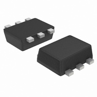
NSBC114EPDXV6T1G ON Semiconductor, NSBC114EPDXV6T1G Datasheet

NSBC114EPDXV6T1G
Specifications of NSBC114EPDXV6T1G
NSBC114EPDXV6T1GOS
NSBC114EPDXV6T1GOSTR
Available stocks
Related parts for NSBC114EPDXV6T1G
NSBC114EPDXV6T1G Summary of contents
Page 1
... Pb−Free Package (Note: Microdot may be in either location) ORDERING INFORMATION Device Package Shipping SOT−563 4 mm pitch NSBC114EPDXV6T1G 4000/Tape & Reel SOT−563 2 mm pitch NSBC114EPDXV6T5G 8000/Tape & Reel †For information on tape and reel specifications, including part orientation and tape sizes, please refer to our Tape and Reel Packaging Specification Brochure, BRD8011/D ...
Page 2
... I E CBO = CEO NSBC114EPDXV6T1G I EBO NSBC124EPDXV6T1G NSBC144EPDXV6T1G NSBC114YPDXV6T1G NSBC114TPDXV6T1G NSBC143TPDXV6T1G NSBC113EPDXV6T1G NSBC123EPDXV6T1G NSBC143EPDXV6T1G NSBC143ZPDXV6T1G NSBC124XPDXV6T1G NSBC123JPDXV6T1G = 0) V (BR)CBO E = 2.0 mA (BR)CEO NSBC114EPDXV6T1G h FE NSBC124EPDXV6T1G NSBC144EPDXV6T1G NSBC114YPDXV6T1G NSBC114TPDXV6T1G NSBC143TPDXV6T1G NSBC113EPDXV6T1G NSBC123EPDXV6T1G NSBC143EPDXV6T1G NSBC143ZPDXV6T1G NSBC124XPDXV6T1G NSBC123JPDXV6T1G http://onsemi.com 2 R1 (kW) R2 (kW ∞ 4.7 ∞ 1.0 1 ...
Page 3
... NSBC123EPDXV6T1G NSBC114TPDXV6T1G NSBC143EPDXV6T1G NSBC143ZPDXV6T1G NSBC124XPDXV6T1G V OL NSBC114EPDXV6T1G NSBC124EPDXV6T1G NSBC114YPDXV6T1G NSBC114TPDXV6T1G NSBC143TPDXV6T1G NSBC113EPDXV6T1G NSBC123EPDXV6T1G NSBC143EPDXV6T1G NSBC143ZPDXV6T1G NSBC124XPDXV6T1G NSBC123JPDXV6T1G NSBC144EPDXV6T1G V OH NSBC114EPDXV6T1G NSBC124EPDXV6T1G NSBC144EPDXV6T1G NSBC114YPDXV6T1G NSBC143TPDXV6T1G NSBC143ZPDXV6T1G NSBC124XPDXV6T1G NSBC123JPDXV6T1G NSBC113EPDXV6T1G NSBC114TPDXV6T1G NSBC123EPDXV6T1G NSBC143EPDXV6T1G http://onsemi.com 3 Min Typ Max Unit Vdc − − 0.25 − ...
Page 4
... Q , − minus sign for Q (PNP) omitted Symbol NSBC114EPDXV6T1G R1 NSBC124EPDXV6T1G NSBC144EPDXV6T1G NSBC114YPDXV6T1G NSBC114TPDXV6T1G NSBC143TPDXV6T1G NSBC113EPDXV6T1G NSBC123EPDXV6T1G NSBC143EPDXV6T1G NSBC143ZPDXV6T1G NSBC124XPDXV6T1G NSBC123JPDXV6T1G R1/R2 NSBC114EPDXV6T1G NSBC124EPDXV6T1G NSBC144EPDXV6T1G NSBC114YPDXV6T1G NSBC114TPDXV6T1G NSBC143TPDXV6T1G NSBC113EPDXV6T1G NSBC123EPDXV6T1G NSBC143EPDXV6T1G NSBC143ZPDXV6T1G NSBC124XPDXV6T1G NSBC123JPDXV6T1G R = 490°C/W qJA 0 50 100 T , AMBIENT TEMPERATURE (°C) A Figure 1 ...
Page 5
TYPICAL ELECTRICAL CHARACTERISTICS − NSBC114EPDXV6T1 NPN TRANSISTOR 0.1 0.01 0.001 COLLECTOR CURRENT (mA) C Figure 2. V versus I CE(sat ...
Page 6
TYPICAL ELECTRICAL CHARACTERISTICS − NSBC114EPDXV6T1 PNP TRANSISTOR -25°C A 0.1 75°C 0. COLLECTOR CURRENT (mA) C Figure 7. V versus I CE(sat ...
Page 7
TYPICAL ELECTRICAL CHARACTERISTICS − NSBC124EPDXV6T1 NPN TRANSISTOR -25°C A 0.1 0.01 0.001 COLLECTOR CURRENT (mA) C Figure 12. V versus I CE(sat ...
Page 8
TYPICAL ELECTRICAL CHARACTERISTICS − NSBC124EPDXV6T1 PNP TRANSISTOR -25°C A 0.1 0. COLLECTOR CURRENT (mA) C Figure 17. V versus I CE(sat ...
Page 9
TYPICAL ELECTRICAL CHARACTERISTICS − NSBC144EPDXV6T1 NPN TRANSISTOR -25°C A 0.1 0. COLLECTOR CURRENT (mA) C Figure 22. V versus I CE(sat) 1 0.8 0.6 0.4 0.2 ...
Page 10
TYPICAL ELECTRICAL CHARACTERISTICS − NSBC144EPDXV6T1 PNP TRANSISTOR -25°C A 0.1 0. COLLECTOR CURRENT (mA) C Figure 27. V versus I CE(sat) 1 0.8 0.6 0.4 0.2 ...
Page 11
TYPICAL ELECTRICAL CHARACTERISTICS − NSBC114YPDXV6T1 NPN TRANSISTOR 0.1 0.01 0.001 COLLECTOR CURRENT (mA) C Figure 32. V versus I CE(sat) 4 3.5 3 2.5 2 1.5 1 0.5 ...
Page 12
TYPICAL ELECTRICAL CHARACTERISTICS − NSBC114YPDXV6T1 PNP TRANSISTOR 0.1 75°C 0.01 0.001 COLLECTOR CURRENT (mA) C Figure 37. V versus I CE(sat) 4.5 4 3.5 3 2.5 2 ...
Page 13
TYPICAL ELECTRICAL CHARACTERISTICS − NSBC114TPDXV6T1 1000 100 1 COLLECTOR CURRENT (mA) C Figure 42. DC Current Gain − PNP TYPICAL ELECTRICAL CHARACTERISTICS − NSBC143TPDXV6T1 1000 100 1 COLLECTOR CURRENT (mA) C Figure 44. DC ...
Page 14
... M *For additional information on our Pb−Free strategy and soldering details, please download the ON Semiconductor Soldering and Mounting Techniques Reference Manual, SOLDERRM/D. ON Semiconductor and are registered trademarks of Semiconductor Components Industries, LLC (SCILLC). SCILLC reserves the right to make changes without further notice to any products herein ...


