NSBC143TPDXV6T1G ON Semiconductor, NSBC143TPDXV6T1G Datasheet - Page 2
NSBC143TPDXV6T1G
Manufacturer Part Number
NSBC143TPDXV6T1G
Description
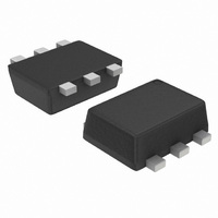
TRANS BR NPN/PNP DUAL 50V SOT563
Manufacturer
ON Semiconductor
Datasheet
1.NSBC124EPDXV6T1G.pdf
(14 pages)
Specifications of NSBC143TPDXV6T1G
Transistor Type
1 NPN, 1 PNP - Pre-Biased (Dual)
Current - Collector (ic) (max)
100mA
Voltage - Collector Emitter Breakdown (max)
50V
Resistor - Base (r1) (ohms)
4.7K
Dc Current Gain (hfe) (min) @ Ic, Vce
160 @ 5mA, 10V
Vce Saturation (max) @ Ib, Ic
250mV @ 300µA, 10mA
Current - Collector Cutoff (max)
500nA
Power - Max
500mW
Mounting Type
Surface Mount
Package / Case
SOT-563, SOT-6
Collector Emitter Voltage V(br)ceo
50V
Continuous Collector Current Ic
100mA
Base Input Resistor R1
4.7kohm
Rf Transistor Case
SOT-563
No. Of Pins
6
Continuous Collector Current Max
100mA
Rohs Compliant
Yes
Lead Free Status / RoHS Status
Lead free / RoHS Compliant
Frequency - Transition
-
Resistor - Emitter Base (r2) (ohms)
-
Other names
NSBC143TPDXV6T1GOS
NSBC143TPDXV6T1GOS
NSBC143TPDXV6T1GOSTR
NSBC143TPDXV6T1GOS
NSBC143TPDXV6T1GOSTR
Available stocks
Company
Part Number
Manufacturer
Quantity
Price
Company:

Part Number:
NSBC143TPDXV6T1G
Manufacturer:
ON Semiconductor
Quantity:
2 750
Company:
Part Number:
NSBC143TPDXV6T1G
Manufacturer:
ON
Quantity:
30 000


DEVICE MARKING AND RESISTOR VALUES
ELECTRICAL CHARACTERISTICS
(T
OFF CHARACTERISTICS
ON CHARACTERISTICS (Note 3)
2. New resistor combinations. Updated curves to follow in subsequent data sheets.
3. Pulse Test: Pulse Width < 300 ms, Duty Cycle < 2.0%
NSBC114EPDXV6T1G
NSBC124EPDXV6T1G
NSBC144EPDXV6T1G
NSBC114YPDXV6T1G
NSBC114TPDXV6T1G (Note 2)
NSBC143TPDXV6T1G (Note 2)
NSBC113EPDXV6T1G (Note 2)
NSBC123EPDXV6T1G (Note 2)
NSBC143EPDXV6T1G (Note 2)
NSBC143ZPDXV6T1G (Note 2)
NSBC124XPDXV6T1G (Note 2)
NSBC123JPDXV6T1G (Note 2)
Collector-Base Cutoff Current (V
Collector-Emitter Cutoff Current (V
Emitter-Base Cutoff Current
(V
Collector-Base Breakdown Voltage (I
Collector-Emitter Breakdown Voltage (Note 3) (I
DC Current Gain
(V
A
EB
CE
= 25°C unless otherwise noted, common for Q
= 6.0 V, I
= 10 V, I
C
C
= 5.0 mA)
= 0)
Device
Characteristic
CB
CE
= 50 V, I
C
= 50 V, I
= 10 mA, I
E
= 0)
B
NSBC124EPDXV6T1G
NSBC144EPDXV6T1G
NSBC143TPDXV6T1G
NSBC123EPDXV6T1G
NSBC143EPDXV6T1G
NSBC143ZPDXV6T1G
NSBC124XPDXV6T1G
NSBC124EPDXV6T1G
NSBC144EPDXV6T1G
NSBC143TPDXV6T1G
NSBC123EPDXV6T1G
NSBC143EPDXV6T1G
NSBC143ZPDXV6T1G
NSBC124XPDXV6T1G
NSBC114EPDXV6T1G
NSBC114YPDXV6T1G
NSBC114TPDXV6T1G
NSBC113EPDXV6T1G
NSBC114EPDXV6T1G
NSBC114YPDXV6T1G
NSBC114TPDXV6T1G
NSBC113EPDXV6T1G
NSBC123JPDXV6T1G
NSBC123JPDXV6T1G
= 0)
C
E
= 2.0 mA, I
1
SOT−563
SOT−563
SOT−563
SOT−563
SOT−563
SOT−563
SOT−563
SOT−563
SOT−563
SOT−563
SOT−563
SOT−563
Package
= 0)
and Q
http://onsemi.com
2
, − minus sign for Q
B
= 0)
2
V
V
Marking
Symbol
(BR)CBO
(BR)CEO
I
I
I
CBO
CEO
h
EBO
11
12
13
14
15
16
30
31
32
33
34
35
FE
1
(PNP) omitted)
Min
160
160
3.0
8.0
50
50
35
60
80
80
15
80
80
80
−
−
−
−
−
−
−
−
−
−
−
−
−
−
R1 (kW)
4.7
1.0
2.2
4.7
4.7
2.2
10
22
47
10
10
22
Typ
100
140
140
350
350
200
150
140
5.0
60
15
30
−
−
−
−
−
−
−
−
−
−
−
−
−
−
−
−
Max
0.18
0.13
100
500
0.5
0.2
0.1
0.2
0.9
1.9
4.3
2.3
1.5
0.2
−
−
−
−
−
−
−
−
−
−
−
−
−
−
R2 (kW)
1.0
2.2
4.7
10
22
47
47
47
47
47
∞
∞
mAdc
nAdc
nAdc
Unit
Vdc
Vdc
Related parts for NSBC143TPDXV6T1G
Image
Part Number
Description
Manufacturer
Datasheet
Request
R

Part Number:
Description:
ON Semiconductor [VOLTAGE REGULATOR]
Manufacturer:
ON Semiconductor
Datasheet:
Part Number:
Description:
357-036-542-201 CARDEDGE 36POS DL .156 BLK LOPRO
Manufacturer:
ON Semiconductor
Datasheet:
Part Number:
Description:
357-036-542-201 CARDEDGE 36POS DL .156 BLK LOPRO
Manufacturer:
ON Semiconductor
Datasheet:
Part Number:
Description:
357-036-542-201 CARDEDGE 36POS DL .156 BLK LOPRO
Manufacturer:
ON Semiconductor
Datasheet:
Part Number:
Description:
357-036-542-201 CARDEDGE 36POS DL .156 BLK LOPRO
Manufacturer:
ON Semiconductor
Datasheet:
Part Number:
Description:
357-036-542-201 CARDEDGE 36POS DL .156 BLK LOPRO
Manufacturer:
ON Semiconductor
Datasheet:
Part Number:
Description:
357-036-542-201 CARDEDGE 36POS DL .156 BLK LOPRO
Manufacturer:
ON Semiconductor
Datasheet:
Part Number:
Description:
357-036-542-201 CARDEDGE 36POS DL .156 BLK LOPRO
Manufacturer:
ON Semiconductor
Datasheet:
Part Number:
Description:
357-036-542-201 CARDEDGE 36POS DL .156 BLK LOPRO
Manufacturer:
ON Semiconductor
Datasheet:
Part Number:
Description:
357-036-542-201 CARDEDGE 36POS DL .156 BLK LOPRO
Manufacturer:
ON Semiconductor
Datasheet:
Part Number:
Description:
357-036-542-201 CARDEDGE 36POS DL .156 BLK LOPRO
Manufacturer:
ON Semiconductor
Datasheet:
Part Number:
Description:
Manufacturer:
ON Semiconductor
Datasheet:
Part Number:
Description:
Manufacturer:
ON Semiconductor
Datasheet:
Part Number:
Description:
Manufacturer:
ON Semiconductor
Datasheet: