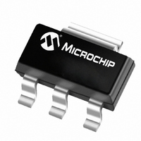
MCP1703-3002E/DB Microchip Technology, MCP1703-3002E/DB Datasheet - Page 5

MCP1703-3002E/DB
Manufacturer Part Number
MCP1703-3002E/DB
Description
LDO Regulator Pos 3V 0.25A 4-Pin (3+Tab) SOT-223 Tube
Manufacturer
Microchip Technology
Type
Linearr
Datasheets
1.SOT89-3EV-VREG.pdf
(28 pages)
2.MCP1703T-3302EMB.pdf
(24 pages)
3.MCP1703-1502EDB.pdf
(26 pages)
Specifications of MCP1703-3002E/DB
Package
4SOT-223
Function
LDO
Number Of Outputs
1
Input Voltage Range
16 to 2.7 V
Output Voltage
3 V
Maximum Output Current
0.25(Min) A
Output Type
Fixed
Accuracy
±2 %
Typical Dropout Voltage @ Current
0.33@250mA|0.525@250mA|0.625@250mA|0.75@250mA V
Operating Temperature
-40 to 125 °C
Polarity
Positive
Regulator Topology
Positive Fixed
Voltage - Output
3V
Voltage - Input
Up to 16V
Voltage - Dropout (typical)
0.625V @ 250mA
Number Of Regulators
1
Current - Output
250mA (Min)
Mounting Type
Surface Mount
Package / Case
SOT-223 (3 leads + Tab), SC-73, TO-261
Input Voltage Max
16 V
Dropout Voltage (max)
0.65 V at 250 mA
Output Current
250 mA
Line Regulation
0.1 % / V
Load Regulation
1 %
Voltage Regulation Accuracy
2 %
Maximum Operating Temperature
+ 125 C
Mounting Style
SMD/SMT
Minimum Operating Temperature
- 40 C
Lead Free Status / RoHS Status
Lead free / RoHS Compliant
Current - Limit (min)
-
Lead Free Status / Rohs Status
Lead free / RoHS Compliant
2.0
Note: Unless otherwise indicated: V
T
Note: Junction Temperature (T
temperature. The test time is small enough such that the rise in Junction temperature over the Ambient temperature is not significant.
FIGURE 2-1:
Voltage.
FIGURE 2-2:
Voltage.
FIGURE 2-3:
Voltage.
2010 Microchip Technology Inc.
A
Note:
= +25°C, V
6.00
5.00
4.00
3.00
2.00
1.00
0.00
6.00
5.00
4.00
3.00
2.00
1.00
0.00
6.00
5.00
4.00
3.00
2.00
1.00
TYPICAL PERFORMANCE CURVES
2
2
6
The graphs and tables provided following this note are a statistical summary based on a limited number of
samples and are provided for informational purposes only. The performance characteristics listed herein
are not tested or guaranteed. In some graphs or tables, the data presented may be outside the specified
operating range (e.g., outside specified power supply range) and therefore outside the warranted range.
+25°C
IN
4
4
0°C
+90°C
= V
8
+130°C
OUT(MAX)
6
6
+90°C
Quiescent Current vs. Input
Quiescent Current vs. Input
Quiescent Current vs. Input
10
Input Voltage (V)
Input Voltage (V)
Input Voltage (V)
8
8
-45°C
0°C
J
-45°C
) is approximated by soaking the device under test to an ambient temperature equal to the desired junction
10
10
12
+ V
+130°C
+130°C
DROPOUT(MAX)
+90°C
12
12
R
-45°C
14
V
I
OUT
OUT
V
I
= 1.8V, C
V
I
OUT
OUT
OUT
OUT
14
14
= 0 µA
0°C
= 1.2V
= 0 µA
= 0 µA
= 2.5V
= 5.0V
16
16
16
+25°C
+25°C
OUT
or 2.7V, whichever is greater.
18
18
18
= 1 µF Ceramic (X7R), C
FIGURE 2-4:
Current.
FIGURE 2-5:
Current.
FIGURE 2-6:
Junction Temperature.
120
100
120
100
3.00
2.50
2.00
1.50
1.00
0.50
0.00
80
60
40
20
80
60
40
20
0
0
-45
0
0
IN
V
V
-20
OUT
IN
= 1 µF Ceramic (X7R), I
= 3.5V
40
50
= 2.5V
Junction Temperature (°C)
5
Load Current (mA)
Load Current (mA)
Ground Current vs. Load
Ground Current vs. Load
Quiescent Current vs.
100
80
V
V
30
V
V
OUT
IN
OUT
IN
= 6.0V
V
V
= 2.7V
= 5.0V
MCP1703
V
V
OUT
IN
= 1.2V
OUT
IN
= 3.5V
= 6.0V
= 2.5V
55
120
150
= 5.0V
DS22049E-page 5
80
I
OUT
L
V
V
160
200
OUT
IN
= 100 µA,
= 2.7V
= 0 mA
105
= 1.2V
200
250
130


