YNV12T05 POWER ONE, YNV12T05 Datasheet
YNV12T05
Specifications of YNV12T05


Related parts for YNV12T05


YNV12T05 Summary of contents
Page 1
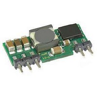
... Description Power-One’s point-of-load converters are recommended for use with regulated bus converters in an Intermediate Bus Architecture (IBA). The YNV12T05 non-isolated DC-DC converters deliver output current in an industry-standard through-hole (SIP) package. The YNV12T05 converters operate from a 9.6 VDC–14 VDC input. ...
Page 2
... The output voltage should not exceed 5.5V (taking into account both the programming and remote sense compensation). 2. Note that start-up time is the sum of turn-on delay time and rise time. 3. The converter ON/OFF pin is left open. MCD10201 Rev. 1.0, 24-Jun-10 YNV12T05 DC-DC Converter Data Sheet Notes Continuous By external resistor, See Trim Table 1 ...
Page 3
... Input Under Voltage Lockout Turn-on Threshold Turn-off Threshold Maximum Input Current Input Stand-by Current (Converter disabled) Input No Load Current (Converter enabled) i Input Reflected-Ripple Current - s MCD10201 Rev. 1.0, 24-Jun-10 YNV12T05 DC-DC Converter Data Sheet Notes 5 ADC Out @ 9.6 VDC 5.0 VDC OUT V = 3.3 VDC OUT ...
Page 4
... Efficiency Additional Notes: 1. See attached waveforms for dynamic response and settling time for different output voltages. MCD10201 Rev. 1.0, 24-Jun-10 YNV12T05 DC-DC Converter Data Sheet Notes Full resistive load @ 3.3 VDC From no load to full load Over line, load and temperature (Fig ...
Page 5
... They should be placed as close as possible to the input pins of the converter. The YNV12T05 has been designed for stable operation with or without external capacitance. Low ESR ceramic capacitors placed as close as possible to the load (minimum 47 μF) are recommended for better transient performance and lower output voltage ripple ...
Page 6
... Vin returns to a specified range. MCD10201 Rev. 1.0, 24-Jun-10 YNV12T05 DC-DC Converter Data Sheet The input voltage must be typically 9.2 V for the converter to turn on. Once the converter has been turned on, it will shut off when the input voltage The Closest drops below typically 8 ...
Page 7
... LFM (0.15 to 2.5 m/s), and vertical MCD10201 Rev. 1.0, 24-Jun-10 YNV12T05 DC-DC Converter Data Sheet and horizontal converter mounting. The airflow during the testing is parallel to the long axis of the converter, going from input pins to output pins. ...
Page 8
... Load Current [Adc] Fig. 5.0V.3: Efficiency vs. load current and input voltage for Vout = 5.0 V converter mounted vertically with air flowing at a rate of 200 LFM (1 m/s) and C. MCD10201 Rev. 1.0, 24-Jun-10 YNV12T05 DC-DC Converter Data Sheet Fig. 5.0V.2: vs ...
Page 9
... Bottom trace: load current (2 A/div.). Co = 100 μF ceramic. Time scale: 20 μs/div. MCD10201 Rev. 1.0, 24-Jun-10 YNV12T05 DC-DC Converter Data Sheet Fig. 5.0V.6: Output voltage ripple (20 mV/div.) at full rated load current into a resistive load with external capacitance 100 μF ceramic and Vin = 12 V for Vout = 5.0 V. Time scale: 1 μ ...
Page 10
... Load Current [Adc] Fig. 3.3V.3: Efficiency vs. load current and input voltage for Vout = 3.3 V converter mounted vertically with air flowing at a rate of 200 LFM (1 m/s) and C. MCD10201 Rev. 1.0, 24-Jun-10 YNV12T05 DC-DC Converter Data Sheet Fig. 3.3V.2: vs ...
Page 11
... Bottom trace: load current (2 A/div.). Co = 100 μF ceramic. Time scale: 20 μs/div. MCD10201 Rev. 1.0, 24-Jun-10 YNV12T05 DC-DC Converter Data Sheet Fig. 3.3V.6: Output voltage ripple (20 mV/div.) at full rated load current into a resistive load with external capacitance 100 μF ceramic and Vin = 12 V for Vout = 3.3 V. Time scale: 1 μ ...
Page 12
... Load Current [Adc] Fig. 2.5V.3: Efficiency vs. load current and input voltage for Vout = 2.5 V converter mounted vertically with air flowing at a rate of 200 LFM (1 m/s) and C. MCD10201 Rev. 1.0, 24-Jun-10 YNV12T05 DC-DC Converter Data Sheet vs. ambient Fig ...
Page 13
... Bottom trace: load current (2 A/div.). Co = 100 μF ceramic. Time scale: 20 μs/div. MCD10201 Rev. 1.0, 24-Jun-10 YNV12T05 DC-DC Converter Data Sheet Fig. 2.5V.6: Output voltage ripple (20 mV/div.) at full rated load current into a resistive load with external capacitance 100 μF ceramic + 1 μF ceramic and Vin = 12 V for Vout = 2.5 V. Time scale: 2 μ ...
Page 14
... Load Current [Adc] Fig. 2.0V.3: Efficiency vs. load current and input voltage for Vout = 2.0 V converter mounted vertically with air flowing at a rate of 200 LFM (1 m/s) and C. MCD10201 Rev. 1.0, 24-Jun-10 YNV12T05 DC-DC Converter Data Sheet vs. ambient Fig ...
Page 15
... Bottom trace: load current (2 A/div.). Co = 100 μF ceramic. Time scale: 20 μs/div. MCD10201 Rev. 1.0, 24-Jun-10 YNV12T05 DC-DC Converter Data Sheet Fig. 2.0V.6: Output voltage ripple (20 mV/div.) at full rated load current into a resistive load with external capacitance 100 μF ceramic and Vin = 12 V for Vout = 2.0 V. Time scale: 1 μ ...
Page 16
... Load Current [Adc] Fig. 1.8V.3: Efficiency vs. load current and input voltage for Vout = 1.8 V converter mounted vertically with air flowing at a rate of 200 LFM (1 m/s) and C. MCD10201 Rev. 1.0, 24-Jun-10 YNV12T05 DC-DC Converter Data Sheet vs. ambient Fig ...
Page 17
... Bottom trace: load current (2 A/div.). Co = 100 μF ceramic. Time scale: 20 μs/div. MCD10201 Rev. 1.0, 24-Jun-10 YNV12T05 DC-DC Converter Data Sheet Fig. 1.8V.6: Output voltage ripple (20 mV/div.) at full rated load current into a resistive load with external capacitance 100 μF ceramic and Vin = 12 V for Vout = 1.8 V. Time scale: 1 μ ...
Page 18
... Load Current [Adc] Fig. 1.5V.3: Efficiency vs. load current and input voltage for Vout = 1.5 V converter mounted vertically with air flowing at a rate of 200 LFM (1 m/s) and C. MCD10201 Rev. 1.0, 24-Jun-10 YNV12T05 DC-DC Converter Data Sheet vs. ambient Fig ...
Page 19
... Bottom trace: load current (2 A/div.). Co = 100 μF ceramic. Time scale: 20 μs/div. MCD10201 Rev. 1.0, 24-Jun-10 YNV12T05 DC-DC Converter Data Sheet Fig. 1.5V.6: Output voltage ripple (20 mV/div.) at full rated load current into a resistive load with external capacitance 100 μF ceramic and Vin = 12 V for Vout = 1.5 V. Time scale: 1 μ ...
Page 20
... Load Current [Adc] Fig. 1.2V.3: Efficiency vs. load current and input voltage for Vout = 1.2 V converter mounted vertically with air flowing at a rate of 200 LFM (1 m/s) and C. MCD10201 Rev. 1.0, 24-Jun-10 YNV12T05 DC-DC Converter Data Sheet vs. ambient Fig ...
Page 21
... Bottom trace: load current (2 A/div.). Co = 100 μF ceramic. Time scale: 20 μs/div. MCD10201 Rev. 1.0, 24-Jun-10 YNV12T05 DC-DC Converter Data Sheet Fig. 1.2V.6: Output voltage ripple (20 mV/div.) at full rated load current into a resistive load with external capacitance 100 μF ceramic and Vin = 12 V for Vout = 1.2 V. Time scale: 1 μ ...
Page 22
... Load Current [Adc] Fig. 1.0V.3: Efficiency vs. load current and input voltage for Vout = 1.0 V converter mounted vertically with air flowing at a rate of 200 LFM (1 m/s) and C. MCD10201 Rev. 1.0, 24-Jun-10 YNV12T05 DC-DC Converter Data Sheet vs. ambient Fig ...
Page 23
... Bottom trace: load current (2 A/div.). Co = 100 μF ceramic. Time scale: 20 μs/div. MCD10201 Rev. 1.0, 24-Jun-10 YNV12T05 DC-DC Converter Data Sheet Fig. 1.0V.6: Output voltage ripple (20 mV/div.) at full rated load current into a resistive load with external capacitance 100 μF ceramic and Vin = 12 V for Vout = 1.0 V. Time scale: 1 μ ...
Page 24
... Load Current [Adc] Fig. 0.7525V.3: Efficiency vs. load current and input voltage for Vout = 0.7525 V converter mounted vertically with air flowing at a rate of 200 LFM (1 m/s) and C. MCD10201 Rev. 1.0, 24-Jun-10 YNV12T05 DC-DC Converter Data Sheet Fig. 0.7525V.2: Available load current vs. ambient temperature and airflow rates for Vout = 0 ...
Page 25
... Bottom trace: load current (2 A/div.). Co = 100 μF ceramic. Time scale: 20 μs/div. MCD10201 Rev. 1.0, 24-Jun-10 YNV12T05 DC-DC Converter Data Sheet Fig. 0.7525V.6: Output voltage ripple (20 mV/div.) at full rated load current into a resistive load with external capacitance 100 μF ceramic and Vin = 12 V for Vout = 0.7525 V. Time scale: 1 μ ...
Page 26
... Y-Series 9.6 – 14 VDC The example above describes P/N YNV12T05: 9.6 – 14 VDC input, through-hole (SIP 0.7525 to 5.5 VDC output, standard enable logic, and RoHS lead-solder-exemption compliancy. Please consult factory regarding availability of a specific version. NUCLEAR AND MEDICAL APPLICATIONS - Power-One products are not designed, intended for use in, or authorized for use as critical components in life support systems, equipment used in hazardous environments, or nuclear control systems without the express written consent of the respective divisional president of Power-One, Inc ...