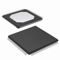
XC2S100E-6TQ144C Xilinx Inc, XC2S100E-6TQ144C Datasheet - Page 32

XC2S100E-6TQ144C
Manufacturer Part Number
XC2S100E-6TQ144C
Description
FPGA Spartan®-IIE Family 100K Gates 2700 Cells 357MHz 0.15um Technology 1.8V 144-Pin TQFP
Manufacturer
Xilinx Inc
Series
Spartan™-IIEr
Datasheet
1.XC2S50E-6TQG144C.pdf
(108 pages)
Specifications of XC2S100E-6TQ144C
Package
144TQFP
Family Name
Spartan®-IIE
Device Logic Cells
2700
Device Logic Units
600
Device System Gates
100000
Maximum Internal Frequency
357 MHz
Typical Operating Supply Voltage
1.8 V
Maximum Number Of User I/os
102
Ram Bits
40960
Number Of Logic Elements/cells
2700
Number Of Labs/clbs
600
Total Ram Bits
40960
Number Of I /o
102
Number Of Gates
100000
Voltage - Supply
1.71 V ~ 1.89 V
Mounting Type
Surface Mount
Operating Temperature
0°C ~ 85°C
Package / Case
144-LQFP
Case
TQFP144
Dc
05+
Lead Free Status / RoHS Status
Contains lead / RoHS non-compliant
Other names
122-1206
Available stocks
Company
Part Number
Manufacturer
Quantity
Price
Company:
Part Number:
XC2S100E-6TQ144C
Manufacturer:
XILINX
Quantity:
339
Company:
Part Number:
XC2S100E-6TQ144C
Manufacturer:
XILINX
Quantity:
3
Part Number:
XC2S100E-6TQ144C
Manufacturer:
XILINX/赛灵思
Quantity:
20 000
Spartan-IIE FPGA Family: DC and Switching Characteristics
Recommended Operating Conditions
DC Characteristics Over Operating Conditions
32
Notes:
1.
2.
3.
Notes:
1.
2.
Symbol
I
V
CCINTQ
V
I
CCOQ
I
I
Functional operation is guaranteed down to a minimum V
V
Minimum and maximum values for V
Input and output measurement threshold is ~50% of V
DRINT
I
With no output current loads, no active input pull-up resistors, all I/O pins 3-stated and floating.
Internal pull-up and pull-down resistors guarantee valid logic levels at unconnected input pins. These pull-up and pull-down resistors
do not provide valid logic levels when input pins are connected to other circuits.
C
RPU
RPD
DRIO
REF
I
CCINT
Symbol
L
IN
V
V
CCINT
T
T
CCO
IN
J
below 1.71V (nominal V
Data retention V
be lost)
Data retention V
lost)
Quiescent V
Quiescent V
V
Input or output leakage current per pin
Input capacitance (sample tested)
Pad pull-up (when selected) @ V
(sample tested)
Pad pull-down (when selected) @ V
REF
current per V
Junction temperature
Supply voltage relative to GND
Supply voltage relative to GND
Input signal transition time
CCINT
CCO
(2)
CCO
CCINT
supply current
CCINT
supply current
REF
voltage (below which configuration data may be
voltage (below which configuration data may
–5%), all delay parameters increase by approximately 3%.
CCO
pin
vary according to the I/O standard selected.
Description
Description
(1)
(1)
IN
(3)
= 0V, V
IN
(1)
(2)
= 3.6V (sample tested)
XC2S50E
XC2S100E
XC2S150E
XC2S200E
XC2S300E
XC2S400E
XC2S600E
TQ, PQ, FG, FT packages
CCO
www.xilinx.com
CCINT
. See
CCO
Commercial
Industrial
Commercial
Industrial
Commercial
Industrial
of 1.62V (Nominal V
= 3.3V
Delay Measurement Methodology, page 41
Commercial
Industrial
Commercial
Industrial
Commercial
Industrial
Commercial
Industrial
Commercial
Industrial
Commercial
Industrial
Commercial
Industrial
(2)
CCINT
1.8 – 5%
1.8 – 5%
–10%). For every 50 mV reduction in
Min
–10
Min
–40
1.5
1.2
1.2
1.2
0
-
-
-
-
-
-
-
-
-
-
-
-
-
-
-
-
-
-
-
-
DS077-3 (v2.3) June 18, 2008
Typ
10
10
10
10
10
10
10
10
12
12
15
15
15
15
-
-
-
-
-
-
-
-
1.8 + 5%
1.8 + 5%
Max
100
250
for specific details.
3.6
3.6
Product Specification
85
Max
0.25
0.25
+10
200
200
200
200
300
300
300
300
300
300
300
300
400
400
20
2
8
-
-
Units
°C
°C
ns
Units
V
V
V
V
mA
mA
mA
mA
mA
mA
mA
mA
mA
mA
mA
mA
mA
mA
mA
mA
mA
μA
μA
pF
V
V
R


