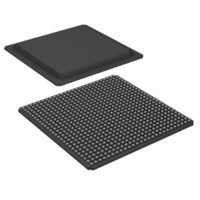
XC2V2000-4FGG676C Xilinx Inc, XC2V2000-4FGG676C Datasheet - Page 27

XC2V2000-4FGG676C
Manufacturer Part Number
XC2V2000-4FGG676C
Description
FPGA Virtex-II™ Family 2M Gates 24192 Cells 650MHz 0.15um/0.12um (CMOS) Technology 1.5V 676-Pin FBGA
Manufacturer
Xilinx Inc
Series
Virtex™-IIr
Datasheet
1.XC2V250-4FGG256C.pdf
(318 pages)
Specifications of XC2V2000-4FGG676C
Package
676FBGA
Family Name
Virtex-IIÂ
Device Logic Units
24192
Device System Gates
2000000
Number Of Registers
21504
Maximum Internal Frequency
650 MHz
Typical Operating Supply Voltage
1.5 V
Maximum Number Of User I/os
456
Ram Bits
1032192
Number Of Labs/clbs
2688
Total Ram Bits
1032192
Number Of I /o
456
Number Of Gates
2000000
Voltage - Supply
1.425 V ~ 1.575 V
Mounting Type
Surface Mount
Operating Temperature
0°C ~ 85°C
Package / Case
676-BBGA
Lead Free Status / RoHS Status
Lead free / RoHS Compliant
Number Of Logic Elements/cells
-
Lead Free Status / RoHS Status
Lead free / RoHS Compliant
Other names
122-1351
Available stocks
Company
Part Number
Manufacturer
Quantity
Price
Company:
Part Number:
XC2V2000-4FGG676C
Manufacturer:
Xilinx Inc
Quantity:
10 000
- Current page: 27 of 318
- Download datasheet (3Mb)
Sum of Products
Each Virtex-II slice has a dedicated OR gate named ORCY,
ORing together outputs from the slices carryout and the ORCY
from an adjacent slice. The ORCY gate with the dedicated
Sum of Products (SOP) chain are designed for implementing
LUTs and MUXCYs can implement large AND gates or
other combinatorial logic functions.
DS031-2 (v3.5) November 5, 2007
Product Specification
4
4
4
4
R
LUT
LUT
LUT
LUT
4
4
4
4
MUXCY
MUXCY
MUXCY
MUXCY
ORCY
Slice 1
Slice 0
V
CC
4
4
4
4
LUT
LUT
LUT
LUT
Figure 26: Wide-Input AND Gate (16 Inputs)
LUT
LUT
LUT
LUT
Figure 26
Figure 25: Horizontal Cascade Chain
MUXCY
MUXCY
MUXCY
MUXCY
ORCY
Slice 2
Slice 3
V
illustrates
CC
“0”
“0”
“0”
CLB
0
0
0
0
MUXCY
MUXCY
MUXCY
MUXCY
www.xilinx.com
V CC
1
1
1
1
4
4
4
4
Slice
Slice
large, flexible SOP chains. One input of each ORCY is con-
nected through the fast SOP chain to the output of the previous
ORCY in the same slice row. The second input is connected to
the output of the top MUXCY in the same slice, as shown in
Figure
LUT and MUXCY resources configured as a 16-input AND
gate.
LUT
LUT
LUT
LUT
OUT
25.
Virtex-II Platform FPGAs: Functional Description
MUXCY
MUXCY
MUXCY
MUXCY
ORCY
Slice 0
Slice 1
V
CC
16
4
4
4
4
LUT
LUT
LUT
LUT
AND
DS031_41_110600
MUXCY
MUXCY
MUXCY
MUXCY
OUT
ORCY
Slice 3
Slice 2
V
CC
CLB
ds031_64_110300
SOP
Module 2 of 4
19
Related parts for XC2V2000-4FGG676C
Image
Part Number
Description
Manufacturer
Datasheet
Request
R

Part Number:
Description:
IC VIRTEX-II FPGA 2M 896-FCBGA
Manufacturer:
Xilinx Inc
Datasheet:

Part Number:
Description:
IC FPGA VIRTEX-II 2M 575-MBGA
Manufacturer:
Xilinx Inc
Datasheet:

Part Number:
Description:
IC FPGA VIRTEX-II 2M 676-FBGA
Manufacturer:
Xilinx Inc
Datasheet:

Part Number:
Description:
IC FPGA VIRTEX-II 2M 676-FBGA
Manufacturer:
Xilinx Inc
Datasheet:

Part Number:
Description:
IC FPGA VIRTEX-II 2M 575-MBGA
Manufacturer:
Xilinx Inc
Datasheet:

Part Number:
Description:
IC FPGA VIRTEX-II 2M 575-MBGA
Manufacturer:
Xilinx Inc
Datasheet:

Part Number:
Description:
IC FPGA VIRTEX-II 2M 896-FBGA
Manufacturer:
Xilinx Inc
Datasheet:

Part Number:
Description:
IC FPGA VIRTEX-II 2M 896-FBGA
Manufacturer:
Xilinx Inc
Datasheet:

Part Number:
Description:
IC FPGA VIRTEX-II 2M 676-FBGA
Manufacturer:
Xilinx Inc
Datasheet:

Part Number:
Description:
IC FPGA VIRTEX-II 2M 676-FBGA
Manufacturer:
Xilinx Inc
Datasheet:

Part Number:
Description:
IC FPGA VIRTEX-II 2M 575-MBGA
Manufacturer:
Xilinx Inc
Datasheet:

Part Number:
Description:
IC FPGA VIRTEX-II 2M 575-MBGA
Manufacturer:
Xilinx Inc
Datasheet:

Part Number:
Description:
IC FPGA VIRTEX-II 2M 896-FBGA
Manufacturer:
Xilinx Inc
Datasheet:

Part Number:
Description:
IC FPGA VIRTEX-II 575PBGA
Manufacturer:
Xilinx Inc
Datasheet:

Part Number:
Description:
IC FPGA VIRTEX-II 896FCBGA
Manufacturer:
Xilinx Inc
Datasheet:


