EMD5DXV6T1 ON Semiconductor, EMD5DXV6T1 Datasheet
EMD5DXV6T1
Specifications of EMD5DXV6T1


Related parts for EMD5DXV6T1


EMD5DXV6T1 Summary of contents
Page 1
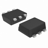
... The BRT eliminates these individual components by integrating them into a single device. In the EMD5DXV6T1 series, two complementary BRT devices are housed in the SOT−563 package which is ideal for low power surface mount applications where board space premium ...
Page 2
... THERMAL CHARACTERISTICS (One Junction Heated) Total Device Dissipation Derate above 25 C Thermal Resistance (Both Junctions Heated) Total Device Dissipation Derate above 25 C Thermal Resistance Junction and Storage Temperature 1. FR−4 @ Minimum Pad EMD5DXV6T1, EMD5DXV6T5 and Q , − minus sign for Rating Characteristic Junction-to-Ambient ...
Page 3
... Collector-Base Breakdown Voltage (I C Collector-Emitter Breakdown Voltage (I = 2.0 mA Current Gain ( 5.0 mA Collector−Emitter Saturation Voltage ( mA Output Voltage ( Output Voltage (off 5 0 Input Resistor Resistor Ratio EMD5DXV6T1, EMD5DXV6T5 = 25 C unless otherwise noted) A Symbol = CBO = CEO = 5.0 mA) I EBO = (BR)CBO = (BR)CEO ...
Page 4
... EMD5DXV6T1, EMD5DXV6T5 250 200 150 100 R = 833 C/W qJA 50 0 − AMBIENT TEMPERATURE ( C) A Figure 1. Derating Curve http://onsemi.com 4 100 150 ...
Page 5
... TYPICAL ELECTRICAL CHARACTERISTICS — EMD5DXV6T1 PNP TRANSISTOR 0.1 0. COLLECTOR CURRENT (mA) C Figure 2. V versus I CE(sat SERIES REVERSE BIAS VOLTAGE (VOLTS) R Figure 4. Output Capacitance EMD5DXV6T1, EMD5DXV6T5 1000 100 = − 100 MHz 0 − 0. Figure 5. Output Current versus Input Voltage http://onsemi.com − 100 ...
Page 6
... TYPICAL ELECTRICAL CHARACTERISTICS — EMD5DXV6T1 NPN TRANSISTOR − 0.1 0. COLLECTOR CURRENT (mA) C Figure 6. V versus I CE(sat) 1 0.8 0.6 0.4 0 REVERSE BIAS VOLTAGE (VOLTS) R Figure 8. Output Capacitance 100 0.1 0 Figure 10. Input Voltage versus Output Current EMD5DXV6T1, EMD5DXV6T5 1000 25 C 100 100 MHz ...
Page 7
... Thermal Clad . Using a board material such as Thermal Clad, an aluminum core board, the power dis- sipation can be doubled using the same footprint. EMD5DXV6T1, EMD5DXV6T5 interface between the board and the package. With the cor- rect pad geometry, the packages will self align when sub- jected to a solder reflow process ...
Page 8
... Phone: 303−675−2175 or 800−344−3860 Toll Free USA/Canada Fax: 303−675−2176 or 800−344−3867 Toll Free USA/Canada Email: orderlit@onsemi.com N. American Technical Support: 800−282−9855 Toll Free USA/Canada EMD5DXV6T1, EMD5DXV6T5 PACKAGE DIMENSIONS SOT−563, 6 LEAD CASE 463A−01 ...