MJE700G ON Semiconductor, MJE700G Datasheet - Page 3
MJE700G
Manufacturer Part Number
MJE700G
Description
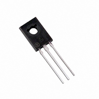
TRANS DARL PNP 4A 60V TO225AA
Manufacturer
ON Semiconductor
Type
Power, Switchr
Specifications of MJE700G
Transistor Type
PNP - Darlington
Current - Collector (ic) (max)
4A
Voltage - Collector Emitter Breakdown (max)
60V
Vce Saturation (max) @ Ib, Ic
2.5V @ 30mA, 1.5A
Current - Collector Cutoff (max)
100µA
Dc Current Gain (hfe) (min) @ Ic, Vce
750 @ 1.5A, 3V
Power - Max
40W
Mounting Type
Through Hole
Package / Case
TO-225-3
Configuration
Single
Transistor Polarity
PNP
Mounting Style
Through Hole
Collector- Emitter Voltage Vceo Max
60 V
Emitter- Base Voltage Vebo
5 V
Collector- Base Voltage Vcbo
60 V
Maximum Dc Collector Current
4 A
Maximum Collector Cut-off Current
100 uA
Maximum Operating Temperature
+ 150 C
Dc Collector/base Gain Hfe Min
100
Minimum Operating Temperature
- 55 C
Current, Gain
100
Current, Input
0.1 ADC
Current, Output
4 ADC
Package Type
TO-225
Polarity
PNP
Power Dissipation
40 W
Primary Type
Si
Voltage, Collector To Emitter, Saturation
3 V
Voltage, Input
5 V
Voltage, Output
60 V
Lead Free Status / RoHS Status
Lead free / RoHS Compliant
Frequency - Transition
-
Lead Free Status / Rohs Status
Lead free / RoHS Compliant
Other names
MJE700GOS


a transistor: average junction temperature and second
breakdown. Safe operating area curves indicate I
limits of the transistor that must be observed for reliable
operation; i.e., the transistor must not be subjected to greater
dissipation than the curves indicate.
R
APPROX
APPROX
+ 8.0 V
B
-12 V
There are two limitations on the power handling ability of
D
V
& R
V
t
DUTY CYCLE = 1.0%
r
1
2
, t
1
, MUST BE FAST RECOVERY TYPE, e.g.:
1N5825 USED ABOVE I
MSD6100 USED BELOW I
f
5.0
3.0
2.0
1.0
0.7
0.5
0.3
0.2
0.1
7.0
0.07
0.05
0.03
0.02
0.01
≤ 10 ns
C
10
0
1.0
0.7
0.5
0.3
0.2
0.1
VARIED TO OBTAIN DESIRED CURRENT LEVELS
5.0
0.01
Figure 2. Switching Times Test Circuit
SINGLE PULSE
0.01
7.0
0.02
0.1
D = 0.5
V
CE
0.05
5.0 ms
BONDING WIRE LIMITED
THERMALLY LIMITED
@ T
SECOND BREAKDOWN LIMITED
0.2
0.03
, COLLECTOR-EMITTER VOLTAGE (VOLTS)
T
J
10
25 ms
B
= 150°C
Figure 5. MJE700 Series
C
≈ 100 mA
B
= 25°C (SINGLE PULSE)
≈ 100 mA
0.05
dc
51
1.0 ms
0.1
For t
and V
to obtain desired test currents.
For NPN test circuit, reverse diode,
polarities and input pulses.
20
R
D
MJE702, 703
MJE700
B
+ 4.0 V
1
d
2
and t
Figure 4. Thermal Response (MJE700, 800 Series)
= 0, R
ACTIVE−REGION SAFE−OPERATING AREA
0.2
30
r
, D
B
≈ 6.0 k
1
and R
id disconnected
0.3
C
TUT
are varied
0.5
50
≈ 150
100 ms
C
- 30 V
V
CC
http://onsemi.com
− V
70
1.0
R
C
CE
SCOPE
100
2.0
t, TIME (ms)
3
3.0
T
pulse limits are valid for duty cycles to 10% provided T
< 150_C. T
At high case temperatures, thermal limitations will reduce
the power that can be handled to values less than the
limitations imposed by second breakdown.
q
q
D CURVES APPLY FOR POWER
PULSE TRAIN SHOWN
READ TIME AT t
T
C
JC
JC
J(pk)
The data of Figures 5 and 6 are based on T
7.0
5.0
3.0
2.0
1.0
0.7
0.5
0.3
0.2
0.1
4.0
2.0
1.0
0.8
0.6
0.4
0.2
10
(t) = r(t) q
is variable depending on conditions. Second breakdown
= 3.12°C/W MAX
5.0
0.04
5.0
- T
C
0.06
= P
JC
7.0
10
J(pk)
(pk)
V
1
CE
q
5.0 ms
0.1
JC
BONDING WIRE LIMITED
THERMALLY LIMITED
@ T
SECOND BREAKDOWN LIMITED
, COLLECTOR-EMITTER VOLTAGE (VOLTS)
may be calculated from the data in Figure 4.
T
(t)
J
10
Figure 3. Switching Times
20
PNP
NPN
= 150°C
Figure 6. MJE800 Series
I
C
C
t
, COLLECTOR CURRENT (AMP)
= 25°C (SINGLE PULSE)
s
30
0.2
dc
50
1.0 ms
20
P
0.4
MJE802, 803
MJE800
V
I
(pk)
C
CC
/I
DUTY CYCLE, D = t
100
B
= 30 V
= 250
0.6
30
t
1
t
2
200
1.0
t
d
I
T
B1
@ V
J
300
= 25°C
t
50
J(pk)
= I
f
BE(off)
B2
1
2.0
/t
100 ms
500
t
2
= 150_C;
r
70
= 0
1000
J(pk)
100
4.0
Related parts for MJE700G
Image
Part Number
Description
Manufacturer
Datasheet
Request
R

Part Number:
Description:
ON Semiconductor [VOLTAGE REGULATOR]
Manufacturer:
ON Semiconductor
Datasheet:
Part Number:
Description:
357-036-542-201 CARDEDGE 36POS DL .156 BLK LOPRO
Manufacturer:
ON Semiconductor
Datasheet:
Part Number:
Description:
357-036-542-201 CARDEDGE 36POS DL .156 BLK LOPRO
Manufacturer:
ON Semiconductor
Datasheet:
Part Number:
Description:
357-036-542-201 CARDEDGE 36POS DL .156 BLK LOPRO
Manufacturer:
ON Semiconductor
Datasheet:
Part Number:
Description:
357-036-542-201 CARDEDGE 36POS DL .156 BLK LOPRO
Manufacturer:
ON Semiconductor
Datasheet:
Part Number:
Description:
357-036-542-201 CARDEDGE 36POS DL .156 BLK LOPRO
Manufacturer:
ON Semiconductor
Datasheet:
Part Number:
Description:
357-036-542-201 CARDEDGE 36POS DL .156 BLK LOPRO
Manufacturer:
ON Semiconductor
Datasheet:
Part Number:
Description:
357-036-542-201 CARDEDGE 36POS DL .156 BLK LOPRO
Manufacturer:
ON Semiconductor
Datasheet:
Part Number:
Description:
357-036-542-201 CARDEDGE 36POS DL .156 BLK LOPRO
Manufacturer:
ON Semiconductor
Datasheet:
Part Number:
Description:
357-036-542-201 CARDEDGE 36POS DL .156 BLK LOPRO
Manufacturer:
ON Semiconductor
Datasheet:
Part Number:
Description:
357-036-542-201 CARDEDGE 36POS DL .156 BLK LOPRO
Manufacturer:
ON Semiconductor
Datasheet:
Part Number:
Description:
Manufacturer:
ON Semiconductor
Datasheet:
Part Number:
Description:
Manufacturer:
ON Semiconductor
Datasheet:
Part Number:
Description:
Manufacturer:
ON Semiconductor
Datasheet: