MJH11022G ON Semiconductor, MJH11022G Datasheet - Page 4
MJH11022G
Manufacturer Part Number
MJH11022G
Description
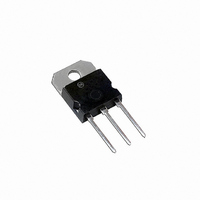
TRANS DARL NPN 15A 250V TO218
Manufacturer
ON Semiconductor
Type
Power, Switchr
Specifications of MJH11022G
Transistor Type
NPN - Darlington
Current - Collector (ic) (max)
15A
Voltage - Collector Emitter Breakdown (max)
250V
Vce Saturation (max) @ Ib, Ic
4V @ 150mA, 15A
Current - Collector Cutoff (max)
1mA
Dc Current Gain (hfe) (min) @ Ic, Vce
400 @ 10A, 5V
Power - Max
150W
Frequency - Transition
3MHz
Mounting Type
Through Hole
Package / Case
SOT-93, TO-218 (Straight Leads)
Configuration
Single
Transistor Polarity
NPN
Mounting Style
SMD/SMT
Collector- Emitter Voltage Vceo Max
250 V
Emitter- Base Voltage Vebo
5 V
Collector- Base Voltage Vcbo
250 V
Maximum Dc Collector Current
15 A
Power Dissipation
150 W
Maximum Operating Temperature
+ 150 C
Continuous Collector Current
15 A
Dc Collector/base Gain Hfe Min
100, 400
Minimum Operating Temperature
- 65 C
Current, Gain
100
Current, Input
0.5 A
Current, Output
15 A
Package Type
SOT-93 (TO-218)
Polarity
NPN
Primary Type
Si
Voltage, Collector To Emitter, Saturation
4 V
Voltage, Input
5 V
Voltage, Output
250 V
Lead Free Status / RoHS Status
Lead free / RoHS Compliant
Other names
MJH11022GOS
Available stocks
Company
Part Number
Manufacturer
Quantity
Price
Company:

Part Number:
MJH11022G
Manufacturer:
ON
Quantity:
30 000
Company:
Part Number:
MJH11022G
Manufacturer:
MOTOROLA
Quantity:
10 000
Part Number:
MJH11022G
Manufacturer:
ON/安森美
Quantity:
20 000


000
000
000
000
000
000
500
200
100
PNP
PNP
30
20
10
0.2
0
0
V
L = 200 mH
I
T
V
R
DUTY CYCLE = 10%
C
CE
0.3
C
BE(off)
BE
20
/I
B1
= 100°C
MJH11017, MJH11018
MJH11019, MJH11020
MJH11021, MJH11022
= 5.0 V
Figure 5. Maximum Rated Reverse Bias
= 47 W
T
≥ 50
C
= 0 - 5.0 V
V
0.5
= 150°C
CE
I
C
Safe Operating Area (RBSOA)
, COLLECTOR CURRENT (AMPS)
60
, COLLECTOR-EMITTER VOLTAGE (VOLTS)
- 55°C
25°C
0.7
1.0
100
140
3.0
180
5.0
220
Figure 6. DC Current Gain
10
http://onsemi.com
260
15
10,000
5000
2000
1000
4
500
200
100
REVERSE BIAS
sustained simultaneously during turn−off, in most cases,
with the base to emitter junction reverse biased. Under these
conditions the collector voltage must be held to a safe level
at or below a specific value of collector current. This can be
accomplished by several means such as active clamping, RC
snubbing, load line shaping, etc. The safe level for these
devices is specified as Reverse Bias Safe Operating Area
and represents the voltage−current conditions during
reverse biased turn−off. This rating is verified under
clamped conditions so that the device is never subjected to
an avalanche mode. Figure 5 gives RBSOA characteristics.
NPN
NPN
0.2
For inductive loads, high voltage and high current must be
V
CE
0.3
= 5.0 V
0.5
I
C
, COLLECTOR CURRENT (AMPS)
0.7
1.0
T
C
- 55°C
= 150°C
25°C
3.0
5.0
7.0
10
15
Related parts for MJH11022G
Image
Part Number
Description
Manufacturer
Datasheet
Request
R

Part Number:
Description:
ON Semiconductor [VOLTAGE REGULATOR]
Manufacturer:
ON Semiconductor
Datasheet:
Part Number:
Description:
357-036-542-201 CARDEDGE 36POS DL .156 BLK LOPRO
Manufacturer:
ON Semiconductor
Datasheet:
Part Number:
Description:
357-036-542-201 CARDEDGE 36POS DL .156 BLK LOPRO
Manufacturer:
ON Semiconductor
Datasheet:
Part Number:
Description:
357-036-542-201 CARDEDGE 36POS DL .156 BLK LOPRO
Manufacturer:
ON Semiconductor
Datasheet:
Part Number:
Description:
357-036-542-201 CARDEDGE 36POS DL .156 BLK LOPRO
Manufacturer:
ON Semiconductor
Datasheet:
Part Number:
Description:
357-036-542-201 CARDEDGE 36POS DL .156 BLK LOPRO
Manufacturer:
ON Semiconductor
Datasheet:
Part Number:
Description:
357-036-542-201 CARDEDGE 36POS DL .156 BLK LOPRO
Manufacturer:
ON Semiconductor
Datasheet:
Part Number:
Description:
357-036-542-201 CARDEDGE 36POS DL .156 BLK LOPRO
Manufacturer:
ON Semiconductor
Datasheet:
Part Number:
Description:
357-036-542-201 CARDEDGE 36POS DL .156 BLK LOPRO
Manufacturer:
ON Semiconductor
Datasheet:
Part Number:
Description:
357-036-542-201 CARDEDGE 36POS DL .156 BLK LOPRO
Manufacturer:
ON Semiconductor
Datasheet:
Part Number:
Description:
357-036-542-201 CARDEDGE 36POS DL .156 BLK LOPRO
Manufacturer:
ON Semiconductor
Datasheet:
Part Number:
Description:
Manufacturer:
ON Semiconductor
Datasheet:
Part Number:
Description:
Manufacturer:
ON Semiconductor
Datasheet:
Part Number:
Description:
Manufacturer:
ON Semiconductor
Datasheet: