MJL21194G ON Semiconductor, MJL21194G Datasheet - Page 2
MJL21194G
Manufacturer Part Number
MJL21194G
Description
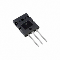
TRANS PWR NPN 16A 250V TO264
Manufacturer
ON Semiconductor
Type
Powerr
Specifications of MJL21194G
Transistor Type
NPN
Current - Collector (ic) (max)
16A
Voltage - Collector Emitter Breakdown (max)
250V
Vce Saturation (max) @ Ib, Ic
4V @ 3.2A, 16A
Current - Collector Cutoff (max)
100µA
Dc Current Gain (hfe) (min) @ Ic, Vce
25 @ 8A, 5V
Power - Max
200W
Frequency - Transition
4MHz
Mounting Type
Through Hole
Package / Case
TO-264-3, TO-3BPL
Transistor Polarity
NPN
Mounting Style
Through Hole
Collector- Emitter Voltage Vceo Max
250 V
Emitter- Base Voltage Vebo
5 V
Maximum Dc Collector Current
16 A
Power Dissipation
200 W
Maximum Operating Temperature
+ 150 C
Continuous Collector Current
16 A
Dc Collector/base Gain Hfe Min
25
Maximum Operating Frequency
4 MHz
Minimum Operating Temperature
- 65 C
Current, Collector
16 A
Current, Gain
8
Frequency
4 MHz
Package Type
TO-3PBL (TO-264)
Polarity
NPN
Primary Type
Si
Resistance, Thermal, Junction To Case
0.7 °C/W
Voltage, Breakdown, Collector To Emitter
250 V
Voltage, Collector To Base
400 V
Voltage, Collector To Emitter
250 V
Voltage, Collector To Emitter, Saturation
4 V
Voltage, Emitter To Base
5 V
Lead Free Status / RoHS Status
Lead free / RoHS Compliant
Other names
MJL21194GOS
Available stocks
Company
Part Number
Manufacturer
Quantity
Price
Company:

Part Number:
MJL21194G
Manufacturer:
ONS
Quantity:
100
Part Number:
MJL21194G
Manufacturer:
ON/安森美
Quantity:
20 000


ELECTRICAL CHARACTERISTICS
OFF CHARACTERISTICS
SECOND BREAKDOWN
ON CHARACTERISTICS
DYNAMIC CHARACTERISTICS
Collector−Emitter Sustaining Voltage
Collector Cutoff Current
Emitter Cutoff Current
Collector Cutoff Current
Second Breakdown Collector Current with Base Forward Biased
DC Current Gain
Base−Emitter On Voltage
Collector−Emitter Saturation Voltage
Total Harmonic Distortion at the Output
Current Gain Bandwidth Product
Output Capacitance
(I
(V
(V
(V
(V
(V
(I
(I
(I
(I
(I
V
(Matched pair h
(I
(V
Figure 1. Typical Current Gain Bandwidth Product
6.5
6.0
5.5
3.5
5.0
4.5
4.0
3.0
C
C
C
C
C
C
C
RMS
CE
CE
CE
CE
CE
CB
0.1
= 100 mAdc, I
= 8 Adc, V
= 16 Adc, I
= 8 Adc, V
= 8 Adc, I
= 16 Adc, I
= 1 Adc, V
= 200 Vdc, I
= 5 Vdc, I
= 250 Vdc, V
= 50 Vdc, t = 1 s (non−repetitive)
= 80 Vdc, t = 1 s (non−repetitive)
= 10 Vdc, I
= 28.3 V, f = 1 kHz, P
T
f
V
test
J
5 V
CE
= 25°C
= 1 MHz
= 10 V
B
CE
CE
CE
B
B
= 0.8 Adc)
C
FE
= 5 Adc)
= 3.2 Adc)
E
= 0)
= 5 Vdc)
= 5 Vdc)
= 10 Vdc, f
B
B
I
= 0, f
BE(off)
C
= 50 @ 5 A/5 V)
= 0)
= 0)
COLLECTOR CURRENT (AMPS)
test
PNP MJL21193
= 1.5 Vdc)
= 1 MHz)
LOAD
test
Characteristic
1.0
= 1 MHz)
= 100 W
(T
C
= 25°C unless otherwise noted)
RMS
h
unmatched
h
matched
FE
FE
10
2
8.0
7.0
6.0
5.0
4.0
3.0
2.0
1.0
0
Figure 2. Typical Current Gain Bandwidth Product
0.1
T
f
test
V
J
Symbol
V
V
CEO(sus)
= 25°C
I
I
I
CE(sat)
= 1 MHz
BE(on)
T
h
C
CEO
EBO
CEX
I
S/b
f
FE
HD
T
ob
I
C
COLLECTOR CURRENT (AMPS)
NPN MJL21194
Min
250
4.0
2.25
25
−
−
−
8
−
−
−
−
−
4
−
1.0
0.08
Typ
0.8
−
−
−
−
−
−
−
−
−
−
−
−
−
V
CE
Max
= 5 V
100
100
100
500
2.2
1.4
75
−
−
−
−
4
−
−
−
10 V
mAdc
mAdc
mAdc
MHz
Unit
Vdc
Adc
Vdc
Vdc
pF
%
10
Related parts for MJL21194G
Image
Part Number
Description
Manufacturer
Datasheet
Request
R

Part Number:
Description:
ON Semiconductor [VOLTAGE REGULATOR]
Manufacturer:
ON Semiconductor
Datasheet:
Part Number:
Description:
357-036-542-201 CARDEDGE 36POS DL .156 BLK LOPRO
Manufacturer:
ON Semiconductor
Datasheet:
Part Number:
Description:
357-036-542-201 CARDEDGE 36POS DL .156 BLK LOPRO
Manufacturer:
ON Semiconductor
Datasheet:
Part Number:
Description:
357-036-542-201 CARDEDGE 36POS DL .156 BLK LOPRO
Manufacturer:
ON Semiconductor
Datasheet:
Part Number:
Description:
357-036-542-201 CARDEDGE 36POS DL .156 BLK LOPRO
Manufacturer:
ON Semiconductor
Datasheet:
Part Number:
Description:
357-036-542-201 CARDEDGE 36POS DL .156 BLK LOPRO
Manufacturer:
ON Semiconductor
Datasheet:
Part Number:
Description:
357-036-542-201 CARDEDGE 36POS DL .156 BLK LOPRO
Manufacturer:
ON Semiconductor
Datasheet:
Part Number:
Description:
357-036-542-201 CARDEDGE 36POS DL .156 BLK LOPRO
Manufacturer:
ON Semiconductor
Datasheet:
Part Number:
Description:
357-036-542-201 CARDEDGE 36POS DL .156 BLK LOPRO
Manufacturer:
ON Semiconductor
Datasheet:
Part Number:
Description:
357-036-542-201 CARDEDGE 36POS DL .156 BLK LOPRO
Manufacturer:
ON Semiconductor
Datasheet:
Part Number:
Description:
357-036-542-201 CARDEDGE 36POS DL .156 BLK LOPRO
Manufacturer:
ON Semiconductor
Datasheet:
Part Number:
Description:
Manufacturer:
ON Semiconductor
Datasheet:
Part Number:
Description:
Manufacturer:
ON Semiconductor
Datasheet:
Part Number:
Description:
Manufacturer:
ON Semiconductor
Datasheet: