2N5038G ON Semiconductor, 2N5038G Datasheet - Page 2
2N5038G
Manufacturer Part Number
2N5038G
Description
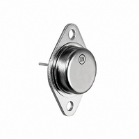
TRANS NPN PWR 20A 90V TO3
Manufacturer
ON Semiconductor
Type
Powerr
Datasheet
1.2N5038G.pdf
(3 pages)
Specifications of 2N5038G
Transistor Type
NPN
Current - Collector (ic) (max)
20A
Voltage - Collector Emitter Breakdown (max)
90V
Vce Saturation (max) @ Ib, Ic
2.5V @ 5A, 20A
Dc Current Gain (hfe) (min) @ Ic, Vce
20 @ 12A, 5V
Power - Max
140W
Mounting Type
Chassis Mount
Package / Case
TO-204, TO-3
Transistor Polarity
NPN
Mounting Style
SMD/SMT
Collector- Emitter Voltage Vceo Max
150 V
Emitter- Base Voltage Vebo
7 V
Maximum Dc Collector Current
20 A
Power Dissipation
140 W
Continuous Collector Current
20 A
Dc Collector/base Gain Hfe Min
20
Current, Collector
20 A
Current, Gain
100
Package Type
TO-204AA (TO-3)
Polarity
NPN
Primary Type
Si
Resistance, Thermal, Junction To Case
1.25 °C/W
Voltage, Breakdown, Collector To Emitter
150 V
Voltage, Collector To Base
150 V
Voltage, Collector To Emitter
90 V
Voltage, Collector To Emitter, Saturation
2.5 V
Voltage, Emitter To Base
7 V
Number Of Elements
1
Collector-emitter Voltage
150V
Collector-base Voltage
150V
Emitter-base Voltage
7V
Collector Current (dc) (max)
20A
Dc Current Gain (min)
20
Operating Temp Range
-65C to 200C
Operating Temperature Classification
Military
Mounting
Through Hole
Pin Count
2 +Tab
Lead Free Status / RoHS Status
Lead free / RoHS Compliant
Current - Collector Cutoff (max)
-
Frequency - Transition
-
Lead Free Status / Rohs Status
Lead free / RoHS Compliant
Other names
2N5038GOS
Available stocks
Company
Part Number
Manufacturer
Quantity
Price

Part Number:
2N5038G
Manufacturer:
ON/安森美
Quantity:
20 000


Î Î Î Î Î Î Î Î Î Î Î Î Î Î Î Î Î Î Î Î Î Î Î Î Î Î Î Î Î Î Î Î Î
Î Î Î Î Î Î Î Î Î Î Î Î Î Î Î Î Î Î Î Î Î Î Î Î Î Î Î Î Î Î Î Î Î
Î Î Î Î Î Î Î Î Î Î Î Î Î Î Î Î Î Î Î Î Î Î
Î Î Î Î Î Î Î Î Î Î Î Î Î Î Î Î Î Î Î Î Î Î
Î Î Î Î Î Î Î Î Î Î Î Î Î Î Î Î Î Î Î Î Î Î Î Î Î Î Î Î Î Î Î Î Î
Î Î Î Î Î Î Î Î Î Î Î Î Î Î Î Î Î Î Î Î Î Î Î Î Î Î Î Î Î Î Î Î Î
Î Î Î Î Î Î Î Î Î Î Î Î Î Î Î Î Î Î Î Î Î Î
Î Î Î Î Î Î Î Î Î Î Î Î Î Î Î Î Î Î Î Î Î Î
Î Î Î Î Î Î Î Î Î Î Î Î Î Î Î Î Î Î Î Î Î Î
Î Î Î Î Î Î Î Î Î Î Î Î Î Î Î Î Î Î Î Î Î Î
Î Î Î Î Î Î Î Î Î Î Î Î Î Î Î Î Î Î Î Î Î Î
Î Î Î Î Î Î Î Î Î Î Î Î Î Î Î Î Î Î Î Î Î Î
Î Î Î Î Î Î Î Î Î Î Î Î Î Î Î Î Î Î Î Î Î Î
Î Î Î Î Î Î Î Î Î Î Î Î Î Î Î Î Î Î Î Î Î Î
Î Î Î Î Î Î Î Î Î Î Î Î Î Î Î Î Î Î Î Î Î Î
Î Î Î Î Î Î Î Î Î Î Î Î Î Î Î Î Î Î Î Î Î Î Î Î Î Î Î Î Î Î Î Î Î
Î Î Î Î Î Î Î Î Î Î Î Î Î Î Î Î Î Î Î Î Î Î Î Î Î Î Î Î Î Î Î Î Î
Î Î Î Î Î Î Î Î Î Î Î Î Î Î Î Î Î Î Î Î Î Î
Î Î Î Î Î Î Î Î Î Î Î Î Î Î Î Î Î Î Î Î Î Î
Î Î Î Î Î Î Î Î Î Î Î Î Î Î Î Î Î Î Î Î Î Î
Î Î Î Î Î Î Î Î Î Î Î Î Î Î Î Î Î Î Î Î Î Î
Î Î Î Î Î Î Î Î Î Î Î Î Î Î Î Î Î Î Î Î Î Î
Î Î Î Î Î Î Î Î Î Î Î Î Î Î Î Î Î Î Î Î Î Î
Î Î Î Î Î Î Î Î Î Î Î Î Î Î Î Î Î Î Î Î Î Î
Î Î Î Î Î Î Î Î Î Î Î Î Î Î Î Î Î Î Î Î Î Î
Î Î Î Î Î Î Î Î Î Î Î Î Î Î Î Î Î Î Î Î Î Î Î Î Î Î Î Î Î Î Î Î Î
Î Î Î Î Î Î Î Î Î Î Î Î Î Î Î Î Î Î Î Î Î Î Î Î Î Î Î Î Î Î Î Î Î
Î Î Î Î Î Î Î Î Î Î Î Î Î Î Î Î Î Î Î Î Î Î
Î Î Î Î Î Î Î Î Î Î Î Î Î Î Î Î Î Î Î Î Î Î
Î Î Î Î Î Î Î Î Î Î Î Î Î Î Î Î Î Î Î Î Î Î
Î Î Î Î Î Î Î Î Î Î Î Î Î Î Î Î Î Î Î Î Î Î Î Î Î Î Î Î Î Î Î Î Î
Î Î Î Î Î Î Î Î Î Î Î Î Î Î Î Î Î Î Î Î Î Î Î Î Î Î Î Î Î Î Î Î Î
Î Î Î Î Î Î Î Î Î Î Î Î Î Î Î Î Î Î Î Î Î Î Î Î Î Î Î Î Î Î Î Î Î
Î Î Î Î Î Î Î Î Î Î Î Î Î Î Î Î Î Î Î Î Î Î Î Î Î Î Î Î Î Î Î Î Î
Î Î Î Î Î Î
Î Î Î Î Î Î
Î Î Î Î Î Î
Î Î Î Î Î Î
3. Indicates JEDEC Registered Data.
4. Pulse Test: Pulse Width v 300, ms, Duty Cycle v 2%.
SWITCHING CHARACTERISTICS
ELECTRICAL CHARACTERISTICS
OFF CHARACTERISTICS
ON CHARACTERISTICS (Note 4)
DYNAMIC CHARACTERISTICS
ORDERING INFORMATION
Collector-Emitter Sustaining Voltage (Note 4)
Collector Cutoff Current
Emitter Cutoff Current
DC Current Gain
Collector-Emitter Saturation Voltage
Base-Emitter Saturation Voltage
Magnitude of Common-Emitter Small-Signal Short-Circuit Forward Current Transfer
Ratio
RESISTIVE LOAD
Rise Time
Storage Time
2N5038
2N5038G
100
0.5
0.2
0.1
50
20
10
5
2
1
(I
(V
(V
(V
(V
(I
(I
(I
1
C
C
C
C
CE
CE
EB
EB
= 200 mAdc, I
= 12 Adc, V
= 20 Adc, I
= 20 Adc, I
Figure 2. Forward Bias Safe Operating Area
= 5 Vdc, I
= 7 Vdc, I
= 140 Vdc, V
= 100 Vdc, V
(I
C
V
= 2 Adc, V
2
CE
Device
Î Î Î Î Î Î Î Î Î Î Î Î Î Î Î Î Î
Î Î Î Î Î Î Î Î Î Î Î Î Î Î Î Î Î
Î Î Î Î Î Î Î Î Î Î Î Î Î Î Î Î Î
Î Î Î Î Î Î Î Î Î Î Î Î Î Î Î Î Î
, COLLECTOR-EMITTER VOLTAGE (VOLTS)
BONDING WIRE LIMIT
THERMAL LIMIT
SECOND BREAKDOWN LIMIT
T
B
B
3
C
C
CE
C
= 5 Adc)
= 5 Adc)
= 25°C
= 0)
= 0)
B
(V
(I
= 5 Vdc)
BE(off)
BE(off)
= 0)
C
CE
CC
5
= 12 Adc, I
= 10 Vdc, f = 5 MHz)
= 30 Vdc)
= 1.5 V)
= 1.5 Vdc, T
7
10
Characteristic
B1
dc
= I
C
(T
B2
20
= 150_C)
C
= 1.2 Adc)
= 25_C unless otherwise noted) (Note 3)
30
50
http://onsemi.com
70
(Pb-Free)
Package
TO-204
TO-204
100
2N5038
2
a transistor: average junction temperature and second
breakdown. Safe operating area curves indicate I
limits of the transistor that must be observed for reliable
operation; i.e., the transistor must not be subjected to greater
dissipation than the curves indicate.
to 10%. At high case temperatures, thermal limitations may
reduce the power that can be handled to values less than the
limitations imposed by second breakdown.
There are two limitations on the power handling ability of
Second breakdown pulse limits are valid for duty cycles
Î Î Î Î Î
Î Î Î Î Î
Î Î Î Î Î
Î Î Î Î Î
Î Î Î Î Î
Î Î Î Î Î
Î Î Î Î Î
Î Î Î Î Î
Î Î Î Î Î
Î Î Î Î Î
Î Î Î Î Î
Î Î Î Î Î
Î Î Î Î Î
Î Î Î Î Î
Î Î Î Î Î
Î Î Î Î Î
Î Î Î Î Î
Î Î Î Î Î
Î Î Î Î Î
Î Î Î Î Î
Î Î Î Î Î
Î Î Î Î Î
Î Î Î Î Î
Î Î Î Î Î
Î Î Î Î Î
Î Î Î Î Î
V
Symbol
V
V
CEO(sus)
I
CE(sat)
BE(sat)
I
|h
h
CEX
EBO
t
FE
t
fe
s
r
|
Î Î Î
Î Î Î
Î Î Î
Î Î Î
Î Î Î
Î Î Î
Î Î Î
Î Î Î
Î Î Î
Î Î Î
Î Î Î
Î Î Î
Î Î Î
Î Î Î
Î Î Î
Î Î Î
Î Î Î
Î Î Î
Î Î Î
Î Î Î
Î Î Î
Î Î Î
Î Î Î
Î Î Î
Î Î Î
Î Î Î
100 Units / Tray
Shipping
Min
90
20
12
-
-
-
-
-
-
-
-
Î Î Î Î
Î Î Î Î
Î Î Î Î
Î Î Î Î
Î Î Î Î
Î Î Î Î
Î Î Î Î
Î Î Î Î
Î Î Î Î
Î Î Î Î
Î Î Î Î
Î Î Î Î
Î Î Î Î
Î Î Î Î
Î Î Î Î
Î Î Î Î
Î Î Î Î
Î Î Î Î
Î Î Î Î
Î Î Î Î
Î Î Î Î
Î Î Î Î
Î Î Î Î
Î Î Î Î
Î Î Î Î
Î Î Î Î
Max
100
2.5
3.3
0.5
1.5
50
10
50
-
5
-
Î Î Î
Î Î Î
Î Î Î
Î Î Î
Î Î Î
Î Î Î
Î Î Î
Î Î Î
Î Î Î
Î Î Î
Î Î Î
Î Î Î
Î Î Î
Î Î Î
Î Î Î
Î Î Î
Î Î Î
Î Î Î
Î Î Î
Î Î Î
Î Î Î
Î Î Î
Î Î Î
Î Î Î
Î Î Î
Î Î Î
C
mAdc
mAdc
Unit
- V
Vdc
Vdc
Vdc
ms
ms
-
-
CE
Related parts for 2N5038G
Image
Part Number
Description
Manufacturer
Datasheet
Request
R

Part Number:
Description:
ON Semiconductor [VOLTAGE REGULATOR]
Manufacturer:
ON Semiconductor
Datasheet:
Part Number:
Description:
357-036-542-201 CARDEDGE 36POS DL .156 BLK LOPRO
Manufacturer:
ON Semiconductor
Datasheet:
Part Number:
Description:
357-036-542-201 CARDEDGE 36POS DL .156 BLK LOPRO
Manufacturer:
ON Semiconductor
Datasheet:
Part Number:
Description:
357-036-542-201 CARDEDGE 36POS DL .156 BLK LOPRO
Manufacturer:
ON Semiconductor
Datasheet:
Part Number:
Description:
357-036-542-201 CARDEDGE 36POS DL .156 BLK LOPRO
Manufacturer:
ON Semiconductor
Datasheet:
Part Number:
Description:
357-036-542-201 CARDEDGE 36POS DL .156 BLK LOPRO
Manufacturer:
ON Semiconductor
Datasheet:
Part Number:
Description:
357-036-542-201 CARDEDGE 36POS DL .156 BLK LOPRO
Manufacturer:
ON Semiconductor
Datasheet:
Part Number:
Description:
357-036-542-201 CARDEDGE 36POS DL .156 BLK LOPRO
Manufacturer:
ON Semiconductor
Datasheet:
Part Number:
Description:
357-036-542-201 CARDEDGE 36POS DL .156 BLK LOPRO
Manufacturer:
ON Semiconductor
Datasheet:
Part Number:
Description:
357-036-542-201 CARDEDGE 36POS DL .156 BLK LOPRO
Manufacturer:
ON Semiconductor
Datasheet:
Part Number:
Description:
357-036-542-201 CARDEDGE 36POS DL .156 BLK LOPRO
Manufacturer:
ON Semiconductor
Datasheet:
Part Number:
Description:
Manufacturer:
ON Semiconductor
Datasheet:
Part Number:
Description:
Manufacturer:
ON Semiconductor
Datasheet:
Part Number:
Description:
Manufacturer:
ON Semiconductor
Datasheet: