TIP33CG ON Semiconductor, TIP33CG Datasheet - Page 3
TIP33CG
Manufacturer Part Number
TIP33CG
Description
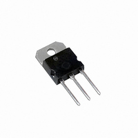
TRANS NPN 10A 100V HI PWR TO-218
Manufacturer
ON Semiconductor
Datasheet
1.TIP33CG.pdf
(4 pages)
Specifications of TIP33CG
Transistor Type
NPN
Current - Collector (ic) (max)
10A
Voltage - Collector Emitter Breakdown (max)
100V
Vce Saturation (max) @ Ib, Ic
4V @ 2.5A, 10A
Current - Collector Cutoff (max)
700µA
Dc Current Gain (hfe) (min) @ Ic, Vce
20 @ 3A, 4V
Power - Max
80W
Frequency - Transition
3MHz
Mounting Type
Through Hole
Package / Case
SOT-93, TO-218 (Straight Leads)
Transistor Polarity
NPN
Mounting Style
SMD/SMT
Collector- Emitter Voltage Vceo Max
100 V
Emitter- Base Voltage Vebo
5 V
Maximum Dc Collector Current
10 A
Power Dissipation
80 W
Maximum Operating Temperature
+ 150 C
Continuous Collector Current
10 A
Dc Collector/base Gain Hfe Min
40
Maximum Operating Frequency
3 MHz
Minimum Operating Temperature
- 65 C
Number Of Elements
1
Collector-emitter Voltage
100V
Collector-base Voltage
100V
Emitter-base Voltage
5V
Collector Current (dc) (max)
10A
Dc Current Gain (min)
40
Frequency (max)
3MHz
Operating Temp Range
-65C to 150C
Operating Temperature Classification
Military
Mounting
Through Hole
Pin Count
3 +Tab
Package Type
SOT-93
Lead Free Status / RoHS Status
Lead free / RoHS Compliant
Other names
TIP33CGOS
Available stocks
Company
Part Number
Manufacturer
Quantity
Price
Company:

Part Number:
TIP33CG
Manufacturer:
ON
Quantity:
30 000


FORWARD BIAS
voltage and current conditions these devices can withstand
during forward bias. The data is based on T
is variable depending on power level. Second breakdown
pulse limits are valid for duty cycles to 10%, and must be
derated thermally for T
The Forward Bias Safe Operating Area represents the
5.0
3.0
2.0
1.0
0.5
0.2
0.1
15
10
1.0
Figure 2. Maximum Rated Forward Bias
T
2.0 3.0
C
V
SECONDARY BREAKDOWN LIMIT
BONDING WIRE LIMIT
THERMAL LIMIT
CE
= 25°C
, COLLECTOR−EMITTER VOLTAGE (VOLTS)
Safe Operating Area
C
5.0 7.0
> 25_C.
10 ms
10
500
200
100
5.0
50
20
10
0.1
dc
1.0 ms
20
TIP33C
TIP33A
C
= 25_C; T
30
Figure 1. DC Current Gain
50
NPN
PNP
300 ms
I
TIP33A, TIP33C
http://onsemi.com
C
, COLLECTOR CURRENT (A)
70
J(pk)
100
3
1.0
REVERSE BIAS
voltage and current conditions these devices can withstand
during reverse biased turn−off. This rating is verified under
clamped conditions so the device is never subjected to an
avalanche mode.
5.0
20
15
10
The Reverse Bias Safe Operating Area represents the
0
0
V
T
Figure 3. Maximum Rated Forward Bias
J
CE
= 25°C
V
= 4.0 V
CE
20
, COLLECTOR−EMITTER VOLTAGE (VOLTS)
Safe Operating Area
10
40
60
L = 200 mH
I
V
T
C
C
BE(off)
/I
B
= 100°C
≥ 5.0
= 0 to 5.0 V
80
100
Related parts for TIP33CG
Image
Part Number
Description
Manufacturer
Datasheet
Request
R

Part Number:
Description:
ON Semiconductor [VOLTAGE REGULATOR]
Manufacturer:
ON Semiconductor
Datasheet:
Part Number:
Description:
357-036-542-201 CARDEDGE 36POS DL .156 BLK LOPRO
Manufacturer:
ON Semiconductor
Datasheet:
Part Number:
Description:
357-036-542-201 CARDEDGE 36POS DL .156 BLK LOPRO
Manufacturer:
ON Semiconductor
Datasheet:
Part Number:
Description:
357-036-542-201 CARDEDGE 36POS DL .156 BLK LOPRO
Manufacturer:
ON Semiconductor
Datasheet:
Part Number:
Description:
357-036-542-201 CARDEDGE 36POS DL .156 BLK LOPRO
Manufacturer:
ON Semiconductor
Datasheet:
Part Number:
Description:
357-036-542-201 CARDEDGE 36POS DL .156 BLK LOPRO
Manufacturer:
ON Semiconductor
Datasheet:
Part Number:
Description:
357-036-542-201 CARDEDGE 36POS DL .156 BLK LOPRO
Manufacturer:
ON Semiconductor
Datasheet:
Part Number:
Description:
357-036-542-201 CARDEDGE 36POS DL .156 BLK LOPRO
Manufacturer:
ON Semiconductor
Datasheet:
Part Number:
Description:
357-036-542-201 CARDEDGE 36POS DL .156 BLK LOPRO
Manufacturer:
ON Semiconductor
Datasheet:
Part Number:
Description:
357-036-542-201 CARDEDGE 36POS DL .156 BLK LOPRO
Manufacturer:
ON Semiconductor
Datasheet:
Part Number:
Description:
357-036-542-201 CARDEDGE 36POS DL .156 BLK LOPRO
Manufacturer:
ON Semiconductor
Datasheet:
Part Number:
Description:
Manufacturer:
ON Semiconductor
Datasheet:
Part Number:
Description:
Manufacturer:
ON Semiconductor
Datasheet:
Part Number:
Description:
Manufacturer:
ON Semiconductor
Datasheet: