MJE5742G ON Semiconductor, MJE5742G Datasheet
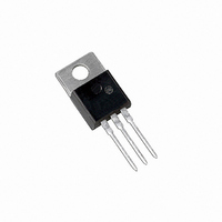
TRANS DARL NPN 8A 400V TO220AB

MJE5742G

Manufacturer Part Number
MJE5742G
Description
TRANS DARL NPN 8A 400V TO220AB
Manufacturer
ON Semiconductor
Type
High Voltage, Powerr
Datasheets

Specifications of MJE5742G

Transistor Type
NPN - Darlington
Current - Collector (ic) (max)
8A
Voltage - Collector Emitter Breakdown (max)
400V
Vce Saturation (max) @ Ib, Ic
3V @ 400mA, 8A
Dc Current Gain (hfe) (min) @ Ic, Vce
200 @ 2A, 5V
Power - Max
2W
Mounting Type
Through Hole
Package / Case
TO-220-3 (Straight Leads)
Configuration
Single
Transistor Polarity
NPN
Mounting Style
Through Hole
Collector- Emitter Voltage Vceo Max
400 V
Emitter- Base Voltage Vebo
8 V
Maximum Dc Collector Current
8 A
Power Dissipation
2 W
Maximum Operating Temperature
+ 150 C
Continuous Collector Current
8 A
Dc Collector/base Gain Hfe Min
200, 50
Minimum Operating Temperature
- 65 C
Current, Gain
400
Current, Input
2.5 A
Current, Output
8 A
Package Type
TO-220AB
Polarity
NPN
Primary Type
Si
Resistance, Thermal, Junction To Ambient
62.5
Voltage, Collector To Emitter, Saturation
3 V
Voltage, Input
8 V
Voltage, Output
400 V
Lead Free Status / RoHS Status
Lead free / RoHS Compliant
Current - Collector Cutoff (max)
-
Frequency - Transition
-
Lead Free Status / Rohs Status
Lead free / RoHS Compliant
Other names
MJE5742GOS

Available stocks

Company
Part Number
Manufacturer
Quantity
Price
Part Number:
MJE5742G
Manufacturer:
ON Semiconductor
Quantity:
1 862
Part Number:
MJE5742G
Manufacturer:
FSC
Quantity:
2 000
MJE5740G, MJE5742G
NPN Silicon Power
Darlington Transistors
for high−voltage power switching in inductive circuits.
Features
Applications
Stresses exceeding Maximum Ratings may damage the device. Maximum
Ratings are stress ratings only. Functional operation above the Recommended
Operating Conditions is not implied. Extended exposure to stresses above the
Recommended Operating Conditions may affect device reliability.
1. Pulse Test: Pulse Width = 5 ms, Duty Cycle ≤ 10%.
*For additional information on our Pb−Free strategy and soldering details, please
MAXIMUM RATINGS
THERMAL CHARACTERISTICS
© Semiconductor Components Industries, LLC, 2011
April, 2011 − Rev. 9
download the ON Semiconductor Soldering and Mounting Techniques
Reference Manual, SOLDERRM/D.
Collector−Emitter Voltage
Emitter−Base Voltage
Collector Current
Base Current
Total Device Dissipation @ T
Derate above 25°C
Total Device Dissipation @ T
Derate above 25°C
Operating and Storage Junction
Temperature Range
Thermal Resistance, Junction−to−Case
Thermal Resistance, Junction−to−Ambient
Maximum Lead Temperature for Soldering
Purposes 1/8″ from Case for 5 Seconds
The MJE5740G and MJE5742G Darlington transistors are designed
These Devices are Pb−Free and are RoHS Compliant*
Small Engine Ignition
Switching Regulators
Inverters
Solenoid and Relay Drivers
Motor Controls
Characteristics
Rating
− Continuous
− Peak (Note 1)
− Continuous
− Peak (Note 1)
C
C
= 25_C
= 25_C
MJE5740
MJE5742
MJE5740
MJE5742
V
Symbol
Symbol
T
CEO(sus)
V
R
R
J
V
I
I
P
P
, T
T
CEV
CM
BM
I
I
qJC
qJA
EB
C
B
D
D
L
stg
−65 to +150
Value
Max
1.25
62.5
300
400
600
800
640
275
2.5
16
16
80
8
8
5
2
1
W/_C
W/_C
_C/W
_C/W
Unit
Unit
Vdc
Vdc
Vdc
Adc
Adc
_C
_C
W
W
See detailed ordering and shipping information in the package
dimensions section on page 2 of this data sheet.
1
2
3
POWER DARLINGTON
MJE574x
G
A
Y
WW
ORDERING INFORMATION
300−400 VOLTS
CASE 221A−09
TRANSISTORS
http://onsemi.com
BASE
TO−220AB
8 AMPERES
STYLE 1
1
80 WATTS
≈ 100
COLLECTOR 2,4
= Device Code
= Pb−Free Package
= Assembly Location
= Year
= Work Week
x = 0 or 2
EMITTER 3
Publication Order Number:
≈ 50
MARKING
DIAGRAM
MJE574xG
AY WW
MJE5740/D

Related parts for MJE5742G

MJE5742G Summary of contents

Page 1

... MJE5740G, MJE5742G NPN Silicon Power Darlington Transistors The MJE5740G and MJE5742G Darlington transistors are designed for high−voltage power switching in inductive circuits. Features • These Devices are Pb−Free and are RoHS Compliant* Applications • Small Engine Ignition • Switching Regulators • ...

Page 2

... The internal Collector−to−Emitter diode can eliminate the need for an external diode to clamp inductive loads. Tests have shown that the Forward Recovery Voltage ( this diode is comparable to that of typical fast recovery rectifiers. f ORDERING INFORMATION Device MJE5740G MJE5742G (T = 25_C unless otherwise noted) C Î Î Î Î Î Î Î Î Î Î Î Î ...

Page 3

SECOND BREAKDOWN DERATING 80 60 THERMAL DERATING 100 T , CASE TEMPERATURE (°C) C Figure 1. Power Derating 2000 150°C 1000 25°C - 55°C 100 ...

Page 4

Table 1. Test Conditions for Dynamic Performance REVERSE BIAS SAFE OPERATING AREA AND INDUCTIVE SWITCHING 1N493 0.001 2N222 W 1 DUTY CYCLE ≤ 10 ≤ ...

Page 5

FORWARD BIAS There are two limitations on the power handling ability of a transistor: average junction temperature and second breakdown. Safe operating area curves indicate I limits of the transistor that must be observed for reliable operation; i.e., the transistor ...

Page 6

... Opportunity/Affirmative Action Employer. This literature is subject to all applicable copyright laws and is not for resale in any manner. PUBLICATION ORDERING INFORMATION LITERATURE FULFILLMENT: Literature Distribution Center for ON Semiconductor P.O. Box 5163, Denver, Colorado 80217 USA Phone: 303−675−2175 or 800−344−3860 Toll Free USA/Canada Fax: 303− ...

Related keywords