TXC100 RFM, TXC100 Datasheet
TXC100
Specifications of TXC100


Related parts for TXC100


TXC100 Summary of contents
Page 1
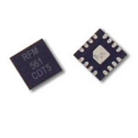
... MHz frequency range. The highly integrated TXC100 includes a complete PLL frequency synthesizer plus an RF power amplifier that require very few external components. The TXC100 is very small in size and features high output power and low current consumption making it ideal for a wide range of short-range wireless applications in the industrial, automotive and consumer markets ...
Page 2
... TXC100 Block Diagram and Typical Application Circuit C 4 XTAL XTAL1 14 C DRV 1 REF /XTAL2 LOGIC EXT CLK0 9 CLK1 10 PIN 4 ENABLE INPUT PIN 16 GND www.RFM.com Email: info@rfm.com ©RF Monolithics, Inc. Mode Input Modulation Mode Select Control (ASK / FSK) Mixer Filter /N /32 5 CLK ...
Page 3
... High (FSK mode): High frequency The Standby Input Pin selects active or low power shutdown/standby mode: If this pin unconnected or logic low, the TXC100 is placed in low current standby mode. If this pin is logic high, the TXC100 is in active mode and ready to transmit 4 Stdby Note: Lowest current consumption is achieved when all configuration pins are logic low. ...
Page 4
... ES Out output, as close as possible to the TXC100 IC to minimize circuit parasitics. The power amplifier side of the resistor should be bypassed with 680 pF and 220 pF capacitors in parallel, as close to the resistor as possible. Power Amplifier - the power amplifier is an open-drain, Class C amplifier designed for a load impedance at PA ohms ...
Page 5
... Test Conditions +25 ° +85 ° +125 ° off, Data=0V (ASK) 50% duty cycle (ASK) mA Data = V (FSK and ASK off, Data=0V (ASK) 50% duty cycle (ASK) Data = V (FSK and ASK µA V Clkout, Load = Clkout, Load = 10 pF 315 MHz Band 433 MHz Band Page TXC100 - 08/18/10 ...
Page 6
... MHz Band 315 MHz Band 433 MHz Band % 315 MHz Band 433 MHz Band dB ASK Mode kHz kHz -40 °C to +85 °C Freq Offset = 100 kHz Freq Offset = 1 MHz into 50Ω matched load DEV[2..0]=111 CW 50% duty cycle Page TXC100 - 08/18/10 ...
Page 7
... Supply Voltage, V Supply Voltage vs Output Power dBm @ 433.92MHz 2.1 2.2 2.3 2.4 2.5 2.6 2.7 2.8 2.9 3 3.1 3.2 3.3 3.4 Supply Voltage, V Output Power vs Supply Current mA @ 433.92MHz Output Power, dBm 3.6 3.8 4 3.5 3.6 3.7 3.8 3 Page TXC100 - 08/18/10 ...
Page 8
... Supply Voltage, V Supply Current and Output Power vs ESout Resistor 433.92MHz 15 Power (dBm Current (mA 0 100 Resistor, Ohms 433.92MHz,FSK,50% DC 433.92MHz,ASK,50 -10 -12 -14 -16 1000 10000 Page TXC100 - 08/18/10 ...
Page 9
... Output Matching When properly matched, the TXC100 can output up to +12 dBm into a 50Ω load. The output is an open-drain configuration which requires a pull-up inductor for biasing. The pull-up inductance serves to provide biasing for the power amplifier and is a high frequency choke to reduce unwanted coupling back into the power supply. Maximum power transfer occurs when the output is closely matched to 250Ω ...
Page 10
... The capacitor may be a variable type or several fixed values may be attempted until an optimal match is reached. The use of a good network analyzer is essential for proper matching and maximum power transfer. For additional information on antenna design see the Application Notes section of our website: http://www.rfm.com/corp/apnotes.htm. Typical Test Circuit www.RFM.com Email: info@rfm.com ©RF Monolithics, Inc. Page TXC100 - 08/18/10 ...
Page 11
... Package Dimensions - 3x3 mm 16-pin TQFN Package (all values in mm) TOP VIEW 3.00 3.00 www.RFM.com Email: info@rfm.com ©RF Monolithics, Inc. BOTTOM VIEW SIDE VIEW 0.0~0.05 0.5 TYP. 0.50 1.50 0.25 0.75 MAX 0.23 TYP. PIN 1 Indicator PIN # 1 0.5 TYP. 0.23 TYP. 0.40 1.50 0.40 Page TXC100 - 08/18/10 ...