TR3003 RFM, TR3003 Datasheet - Page 10
TR3003
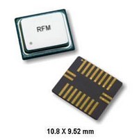
Manufacturer Part Number
TR3003
Description
RF Receiver 2G ASH Transceiver 303.825MHz 115.2kbps
Manufacturer
RFM
Type
Transceiverr
Datasheet
1.TR3003.pdf
(12 pages)
Specifications of TR3003
Package / Case
SM-20L
Operating Frequency
304.025 MHz
Operating Supply Voltage
3.3 V
Maximum Operating Temperature
+ 85 C
Minimum Operating Temperature
- 40 C
Mounting Style
SMD/SMT
Lead Free Status / RoHS Status
Lead free / RoHS Compliant


www.RFM.com
©2008 by RF Monolithics, Inc.
Pin
10
12
13
14
11
8
9
TXMOD
LPFADJ
PRATE
THLD2
THLD1
E-mail: info@rfm.com
Name
GND2
RREF
The transmitter RF output voltage is proportional to the input current to this pin. A series resistor is used to adjust the peak
transmitter output voltage. 1.5 dBm output power requires about 250 µA of input current. In the ASK mode, minimum output
power occurs when the modulation driver sinks about 10 µA of current from this pin. In the OOK mode, input signals less than
220 mV completely turn the transmitter oscillator off. Internally, this pin appears to be a diode in series with a small resistor.
Peak transmitter output power P
A ±5% resistor value is recommended. In the OOK mode, this pin is usually driven with a logic-level data input (unshaped
data pulses). OOK modulation is practical for data pulses of 30 µs or longer. In the ASK mode, this pin accepts analog mod-
ulation (shaped or unshaped data pulses). ASK modulation is practical for data pulses 8.7 µs or longer. The resistor driving
this pin must be low in the receive and power-down (sleep) modes. Please refer to the ASH Transceiver Designer’s Guide for
additional information on modulation techniques.
This pin is the receiver low-pass filter bandwidth adjust. The filter bandwidth is set by a resistor R
ground. The resistor value can range from 330 K to 820 ohms, providing a filter 3 dB bandwidth f
The resistor value is determined by:
A ±5% resistor should be used to set the filter bandwidth. This will provide a 3 dB filter bandwidth between f
with variations in supply voltage, temperature, etc. The filter provides a three-pole, 0.05 degree equiripple phase response.
The peak drive current available from RXDATA increases in proportion to the filter bandwidth setting.
GND2 is an IC ground pin. It should be connected to GND1 by a short, low inductance trace.
RREF is the external reference resistor pin. A 100 K reference resistor is connected between this pin and ground. A ±1%
resistor tolerance is recommended. It is important to keep the total capacitance between ground, Vcc and this node to less
than 5 pF to maintain current source stability. If THLD1 and/or THDL2 are connected to RREF through resistor values less
that 1.5 K, their node capacitance must be added to the RREF node capacitance and the total should not exceed 5 pF.
THLD2 is the “dB-below-peak” data slicer (DS2) threshold adjust pin. The threshold is set by a 0 to 200 K resistor R
between this pin and RREF. Increasing the value of the resistor decreases the threshold below the peak detector value
(increases difference) from 0 to 120 mV. For most applications, this threshold should be set at 6 dB below peak, or 60 mV for
a 50%-50% RF amplifier duty cycle. The value of the THLD2 resistor is given by:
A ±1% resistor tolerance is recommended for the THLD2 resistor. Leaving the THLD2 pin open disables the dB-below-peak
data slicer operation.
The THLD1 pin sets the threshold for the standard data slicer (DS1) through a resistor R
increased by increasing the resistor value. Connecting this pin directly to RREF provides zero threshold. The value of the
resistor depends on whether THLD2 is used. For the case that THLD2 is not used, the acceptable range for the resistor is 0
to 100 K, providing a THLD1 range of 0 to 90 mV. The resistor value is given by:
For the case that THLD2 is used, the acceptable range for the THLD1 resistor is 0 to 200 K, again providing a THLD1 range
of 0 to 90 mV. The resistor value is given by:
A ±1% resistor tolerance is recommended for the THLD1 resistor. Note that a non-zero DS1 threshold is required for proper
AGC operation.
The interval between the falling edge of an ON pulse to the first RF amplifier and the rising edge of the next ON pulse to the
first RF amplifier t
5 µs with a resistor in the range of 51 K to 2000 K. The value of R
A ±5% resistor value is recommended. When the PWIDTH pin is connected to Vcc through a 1 M resistor, the RF amplifiers
operate at a nominal 50%-50% duty cycle, facilitating high data rate operation. In this case, the period t
of ON pulses to the first RF amplifier is controlled by the PRATE resistor over a range of 0.1 to 1.1 µs using a resistor of 11 K
to 220 K. In this case the value of R
A ±5% resistor value should also be used in this case. Please refer to the ASH Transceiver Designer’s Guide for additional
amplifier duty cycle information. It is important to keep the total capacitance between ground, Vcc and this pin to less than 5
pF to maintain stability.
P
R
R
R
R
R
R
O
LPF
TH2
TH1
TH1
PR
PR
= 24*(I
= 404* t
= 198* t
= 1445/ f
= 1.67*V, where R
= 1.11*V, where R
= 2.22*V, where R
PRI
TXM
PRI
PRC
is set by a resistor R
)
LPF
2
, where P
+ 10.5, where t
- 8.51, where t
, where R
TH1
TH2
TH1
O
O
for a 3 Vdc supply voltage is approximately:
is in mW, and the peak modulation current ITXM is in mA
is in kilohms and the threshold V is in mV
LPF
is in kilohms and the threshold V is in mV
is in kilohms and the threshold V is in mV
PR
PRI
is given by:
PRC
is in kilohms, and f
PR
is in µs, and R
is in µs and R
between this pin and ground. The interval t
Description
PR
PR
LPF
is in kilohms
is in kilohms
is in kHz
PR
is given by:
PRI
TH1
can be adjusted between 0.1 and
to RREF. The threshold is
LPF
LPF
from 4.5 kHz to 1.8 MHz.
between this pin and
PRC
from start-to-start
LPF
and 1.3* f
TR3003 - 4/4/08
Page 10 of 12
TH2
LPF
Related parts for TR3003
Image
Part Number
Description
Manufacturer
Datasheet
Request
R

Part Number:
Description:
ASH RX 115.2 KBPS 433.92 MHZ
Manufacturer:
RFM
Datasheet:

Part Number:
Description:
RFIC TRANCEIVER MULTI-CHANNEL FS
Manufacturer:
RFM
Datasheet:

Part Number:
Description:
ASH TX 115.2 KBPS 433.92 MHZ
Manufacturer:
RFM
Datasheet:
Part Number:
Description:
Filters 1602MHz BW=61MHz
Manufacturer:
RFM
Datasheet:

Part Number:
Description:
RESONATOR, SM3030-6
Manufacturer:
RFM
Datasheet:

Part Number:
Description:
RESONATOR, SM3030-6
Manufacturer:
RFM
Datasheet:

Part Number:
Description:
RESONATOR, SM3030-6
Manufacturer:
RFM
Datasheet:

Part Number:
Description:
RESONATOR, SM5035-4
Manufacturer:
RFM
Datasheet:
Part Number:
Description:
RESONATOR 418MHZ SM5035-4
Manufacturer:
RFM
Datasheet:
Part Number:
Description:
RESONATOR 315 MHZ SMD
Manufacturer:
RFM
Datasheet:

Part Number:
Description:
10-Terminal Ceramic Surface-Mount Case 7 x 5 mm Nominal Footprint
Manufacturer:
RFM [RF Monolithics, Inc]
Datasheet:
Part Number:
Description:
QUAD-BAND GSM850/GSM/DCS/PCS POWER AMP MODULE
Manufacturer:
RFM [RF Monolithics, Inc]
Datasheet:
Part Number:
Description:
402 to 405 MHz Medical Band Front-end Filter
Manufacturer:
RFM [RF Monolithics, Inc]
Datasheet:
Part Number:
Description:
674.03 MHz SAW Resonator
Manufacturer:
RFM [RF Monolithics, Inc]
Datasheet: