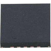
T7024-PGPM80 Atmel, T7024-PGPM80 Datasheet

T7024-PGPM80
Specifications of T7024-PGPM80
Related parts for T7024-PGPM80
T7024-PGPM80 Summary of contents
Page 1
... Few External Components • QFN20 Package with Extended Performance 1. Description The T7024 is a monolithic SiGe transmit/receive front-end IC with power amplifier, low-noise amplifier and T/R switch driver especially designed for operation in ® TDMA systems like Bluetooth and WDCT. Due to the ramp-control feature and a very low quiescent current, an external switch transistor for V is not required ...
Page 2
... GND 19 V1_PA 20 PA_IN Slug GND T7024 V3_PA_OUT SWITCH_OUT 11 5 V3_PA_OUT R_SWITCH 12 4 V3_PA_OUT T7024 GND RX_ON 14 2 RAMP LNA_OUT Function Low-noise amplifier output RX active high Power-up active high Resistor to GND sets the PIN diode current Switched current output for PIN diode ...
Page 3
... Standby current Ambient temperature 4533I–BLURF–01/09 Symbol stg P inLNA P inPA Symbol R thJA Symbol Min. Typ. V 2.7 3 2.7 3 165 S_standby T –25 +25 amb T7024 Value Unit 6 V 150 °C –40 to +125 °C 5 dBm 10 dBm Value Unit 27 K/W Max. Unit 4 µA +85 °C 3 ...
Page 4
... VSWR = 10:1 (all phases) 10s With external matching network, load impedance Low-noise amplifier shall be unconditionally stable. 4. With external matching components. 5. LNA gain can be adjusted with RX_ON voltage according to 1.4V the T/R switch driver switches to TX mode. T7024 4 = 3.0V 25°C S amb ...
Page 5
... Please note, that for RX_ON below LNA Antenna Switch Driver off off off off on off on off off on off on on off on off T7024 Max. Unit 10 µA 2.5 GHz 19 dB 2.3 dB –6 dBm –13 dBm 2:1 2 LNA 0 µA 0.2 µA Operation Mode standby ...
Page 6
... Typical Operating Characteristics Figure 9-1. Figure 9-2. Figure 9-3. T7024 6 LNA: Gain and Noise Figure versus Frequency 25 20 Gain 2000 2200 2400 Frequency (MHz) LNA: NF and Gain versus Temperature 2.5 2.0 NF 1.5 1.0 0.5 0.0 -0.5 Gain -1.0 -1.5 -2.0 -2.5 ...
Page 7
... Pout 160 f = 2.4 GHz V = 1.8V ramp 130 dBm inPA 100 3.9 4.3 4.7 250 200 Pout 150 100 f = 2.4 GHz dBm inPA 50 0 1.8 2.0 (V) 300 250 PAE 200 150 100 f = 2.4 GHz V = 1.8V ramp dBm 50 inPA 0 -10 0 -10 T7024 7 ...
Page 8
... Figure 9-7. Figure 9-8. Figure 9-9. T7024 8 PA: Output Power and PAE versus Frequency 50 PAE 40 I_S_TX 30 Pout 2400 2420 2440 Frequency (MHz) LNA: Supply Current versus Temperature 8.0 7.8 7.6 7.4 7.2 7.0 6.8 6.6 6.4 6.2 6.0 -40 -20 0 Temperature ( PA: P versus V ...
Page 9
... Figure 9-10. LNA Gain (dB) versus RX_ON (V) 10. Input/Output Circuits Figure 10-1. Input Circuit PA_IN/V1_PA Figure 10-2. Input Circuit RAMP/V1_PA 4533I–BLURF–01/ -10 -15 -20 -25 1 1.5 2 RX_ON (V) V1_PA PA_IN GND V1_PA RAMP T7024 2 ...
Page 10
... Figure 10-3. Input Circuit V2_PA Figure 10-4. Input/Output Circuit V3_PA_OUT Figure 10-5. Input Circuit SWITCH_OUT/R_SWITCH T7024 10 V2_PA GND V3_PA_OUT GND V1_PA SWITCH_OUT R_SWITCH GND 4533I–BLURF–01/09 ...
Page 11
... Figure 10-6. Input Circuit LNA_IN/VS_LNA Figure 10-7. Input Circuit PU/RX_ON Figure 10-8. Output Circuit LNA_OUT 4533I–BLURF–01/09 VS_LNA LNA_IN GND VS_LNA LNA_IN / PU VS_LNA LNA_OUT GND T7024 11 ...
Page 12
... Figure 10-9. Typical Application T7024 T7024 12 LNA_OUT PA_IN 2 PX_ON 2 T7024 selected with DIL-switch Var Pin diode replaced by LED on application board 1.8 pF Switch_OUT LNA_IN V1_PA V2_PA 3 PA_RAMP 14 13 harm. termination VS_LNA V3_PA PA_OUT blocking capacitors depending on application 4533I–BLURF–01/09 ...
Page 13
... Issue: 1; 19.12.02 4533I–BLURF–01/09 Package Remarks Taped and reeled QFN20 Pb free, halogen free Taped and reeled QFN20 Pb free, halogen free QFN20 Evaluation board QFN 0.9 ±0.1 +0 0.05 -0. T7024 MOQ 1500 pcs. 6000 pcs 3 technical drawings according to DIN 5 specifications 6 0.65 nom. 2.6 13 ...
Page 14
... Recommended PCB Land Pattern Figure 13-1. Recommended PCB Land Pattern Table 13-1. 14. Revision History Please note that the following page numbers referred to in this section refer to the specific revision mentioned, not to this document. Revision No. 4533I-BLURF-01/09 4533H-BLURF-07/07 T7024 Recommended PCB Land Pattern Signs Sign Description ...
Page 15
... Disclaimer: The information in this document is provided in connection with Atmel products. No license, express or implied, by estoppel or otherwise, to any intellectual property right is granted by this document or in connection with the sale of Atmel products. EXCEPT AS SET FORTH IN ATMEL’S TERMS AND CONDI- TIONS OF SALE LOCATED ON ATMEL’S WEB SITE, ATMEL ASSUMES NO LIABILITY WHATSOEVER AND DISCLAIMS ANY EXPRESS, IMPLIED OR STATUTORY WARRANTY RELATING TO ITS PRODUCTS INCLUDING, BUT NOT LIMITED TO, THE IMPLIED WARRANTY OF MERCHANTABILITY, FITNESS FOR A PARTICULAR PURPOSE, OR NON-INFRINGEMENT ...


