VG101-F TriQuint, VG101-F Datasheet - Page 4
VG101-F
Manufacturer Part Number
VG101-F
Description
RF Amplifier 50-2200MHz +40dBm OIP3
Manufacturer
TriQuint
Type
Gain Amplifierr
Datasheet
1.VG101-PCB.pdf
(4 pages)
Specifications of VG101-F
Operating Frequency
700 MHz to 1000 MHz
P1db
22 dBm
Noise Figure
3.5 dB
Operating Supply Voltage
5 V
Supply Current
150 mA
Maximum Operating Temperature
+ 220 C
Mounting Style
SMD/SMT
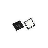
Package / Case
QFN-28
Number Of Channels
1 Channel
Lead Free Status / RoHS Status
Lead free / RoHS Compliant
Other names
1066892
Available stocks
Company
Part Number
Manufacturer
Quantity
Price

Part Number:
VG101-F
Manufacturer:
WJ
Quantity:
20 000


TriQuint Semiconductor, Inc •
VG101
Cellular-band Variable Gain Amplifier
This package is lead-free/RoHS-compliant. The plating material on the pins is annealed matte tin over copper. It is compatible with both
Mounting Configuration / Land Pattern
lead-free (maximum 260 °C reflow temperature) and leaded (maximum 245 °C reflow temperature) soldering processes.
YYWWAaXXXX
Phone +1-503-615-9000 • FAX: +1-503-615-8900
Outline Drawing
VG101-F Mechanical Information
• e-mail: info-sales@tqs.com • Web site: www.TriQuint.com
Specifications and information are subject to change without notice
The component will be lasermarked with a
“VG101F” designator followed by 10-digit
numeric lot code. The “YY” represents the last
digit of the year the part was manufactured,
“WW” represents the workweek, the “Aa” is
vendor code and “XXXX” is an auto-generated
number.
Tape and reel specifications for this part will be
located on the website in the “Application
Notes” section.
ESD Rating: Class 1B
Value:
Test:
Standard:
ESD Rating: Class IV
Value:
Test:
Standard:
MSL Rating: Level 2 at +260°C convection reflow
Standard:
ESD / MSL Information
Functional Pin Layout
The even numbered pins are hard grounded
RF IN
GND
GND
GND
GND
GND
GND
Product Marking
RF Output / DC bias
to the backside paddle internally.
Interstage Match
10
11
12
13
14
8
9
Gain Control
No Connect
Passes
Human Body Model (HBM)
JEDEC Standard JESD22-A114
Passes
Charged Device Model (CDM)
JEDEC Standard JESD22-C101
JEDEC Standard J-STD-020
Function
RF Input
Ground
15
7
Attenuator
Variable
16
6
500V to <1000V
1000V to <2000V
17
5
18
4
19
Backside copper
Page 4 of 4
3
All other pins
Amp
20
Pin No
2
7, 19
21
25
11
5
21
1
28
27
26
25
24
23
22
August 2009
GND
GND
GND
RF OUT
GND
GND
GND
Related parts for VG101-F
Image
Part Number
Description
Manufacturer
Datasheet
Request
R

Part Number:
Description:
WiFi / 802.11 Modules & Development Tools 900MHz Eval Brd 16dB Gain
Manufacturer:
TriQuint
Datasheet:

Part Number:
Description:
Manufacturer:
TriQuint
Datasheet: