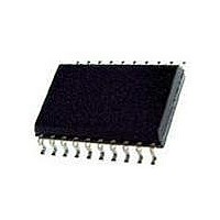
ATA5760N-TGQY Atmel, ATA5760N-TGQY Datasheet - Page 29

ATA5760N-TGQY
Manufacturer Part Number
ATA5760N-TGQY
Description
RF Receiver ASK/FSK Receiver 868 MHz
Manufacturer
Atmel
Type
UHF ASK/FSK Receiversr
Datasheet
1.ATA5760N-TGSY.pdf
(41 pages)
Specifications of ATA5760N-TGQY
Package / Case
SOIC-20
Operating Frequency
928 MHz
Operating Supply Voltage
5 V
Maximum Operating Temperature
+ 105 C
Minimum Operating Temperature
- 40 C
Mounting Style
SMD/SMT
Operating Temperature (min)
-40C
Operating Temperature (max)
105C
Operating Temperature Classification
Industrial
Operating Supply Voltage (min)
4.5V
Operating Supply Voltage (typ)
5V
Operating Supply Voltage (max)
5.5V
Lead Free Status / RoHS Status
Lead free / RoHS Compliant
14. Data Interface
4896D–RKE–08/08
Bit 15 is followed by the equivalent time window t9. During this window, the equivalence
acknowledge pulse t8 (E_Ack) occurs if the just programmed mode word is equivalent to the
mode word that was already stored in that register. E_Ack should be used to verify that the
mode word was correctly transferred to the register. The register must be programmed twice in
that case.
Programming of a register is possible both in sleep-mode and in active-mode of the receiver.
During programming, the LNA, LO, lowpass filter IF-amplifier and the FSK/ASK Manchester
demodulator are disabled.
The programming start pulse t1 initiates the programming of the configuration registers. If bit 1 is
set to ’1’, it represents the OFF command to set the receiver back to polling mode at the same
time. For the length of the programming start pulse t1, the following convention should be
considered:
Programming respectively OFF command is initiated if the receiver is not in reset mode. If the
receiver is in reset mode, programming respectively Off command is not initiated and the reset
marker RM is still present at pin DATA.
This period is generally used to switch the receiver to polling mode or to start the programming
of a register. In reset condition, RM is not cancelled by accident.
Programming respectively OFF command is initiated in any case. The registers OPMODE and
LIMIT are set to the default values. RM is cancelled if present.
This period is used if the connected microcontroller detected RM. If the receiver operates in
default mode, this time period for t1 can generally be used.
Note that the capacitive load at pin DATA is limited.
The data interface (see
be connected via the pull-up resistor R
The applicable pull-up resistor R
selected BR_range (see
Table 14-1.
• t1(min) < t1 < 5632 T
• t1 > 7936
t1(min) is the minimum specified value for the relevant BR_Range
C
C
L
L
100pF
-
1nF
Applicable R
T
Clk
Figure 13-2 on page
Clk
Table
:
pup
BR_range
14-1).
B0
B1
B2
B3
B0
B1
B2
B3
pup
depends on the load capacity C
pup
up to 20V and is short-circuit-protected.
28) is designed for automotive requirements. It can
ATA5760/ATA5761
Applicable R
1.6 k to 470 k
1.6 k to 220 k
1.6 k to 120 k
1.6 k to 5.6 k
1.6 k to 47 k
1.6 k to 22 k
1.6 k to 12 k
1.6 k to 56 k
L
at pin DATA and the
pup
29


