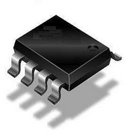
ATA6661-TAQJ Atmel, ATA6661-TAQJ Datasheet

ATA6661-TAQJ
Specifications of ATA6661-TAQJ
Available stocks
Related parts for ATA6661-TAQJ
ATA6661-TAQJ Summary of contents
Page 1
... ESD HBM LIN Bus Pin and Supply VS Pin 1. Description The ATA6661 is a fully integrated LIN transceiver according to the LIN specification 2.0. It interfaces the LIN protocol handler and the physical layer. The device is designed to handle the low-speed data communication in vehicles, e.g., in convenience electronics ...
Page 2
... GND Ground 6 LIN LIN bus line input/output 7 VS Battery supply Battery related inhibit output for controlling an external voltage regulator; active high after a wake-up 8 INH request ATA6661 2 Receiver - + Wake up bus timer TXD Slew rate control Time-out timer Control unit Wake-up Sleep mode ...
Page 3
... After switching on V INHIBIT is switched on. The supply current in sleep mode is typically 10 µA. 3.2 Ground Pin (GND) The ATA6661 is neutral on the LIN pin in case of a GND disconnection able to handle a ground shift for V 3.3 Bus Pin (LIN) A low-side driver with internal current limitation and thermal shutdown as well as an internal pull-up resistor according to LIN specification 2.0 are implemented. The voltage range is from – ...
Page 4
... Wake-up events from sleep mode: • LIN bus • EN pin • WAKE pin Figure 3-1 on page ATA6661 4 with a weak pull-up current source. The device can transmit only after being S “Inhibit Output Pin (INH)” rises from zero), the pin INH switches automatically to the V ...
Page 5
... The voltage threshold for a wake-up signal is 3V below the VS voltage with ) and the internal termination resistor is switched on. The local S Figure 3-3 on page and Figure 3-3). level. The microcontroller of the application will S ) ensures that no tran- WAKE 7). ATA6661 ), WAKE is S Fig- ), WAKE Figure 3 ...
Page 6
... LIN physical layer according to this revision can be mixed with LIN physical layer nodes, which are according to older versions (i.e. LIN 1.0, LIN 1.1, LIN 1.2, LIN 1.3), without any restrictions. A higher ratio of nodes according to this LIN physical layer specification or the one of revision 2.0 will result in a higher transmission reliability. ATA6661 6 Unpowered Mode V ...
Page 7
... Microcontroller start-up time delay State change Low or floating High or floating TXD strong pull-down Wake filtering time t WAKE Off state Regulator wake-up time delay Node in sleep state Microcontroller start-up time delay ATA6661 High Low On state Node in Operation EN High High Low High weak pull-down ...
Page 8
... CDM ESD STM 5.3.1-1999 - All pins FCDM ESD STM 5.3.1- All pins MM JEDEC A115A - All pins Junction temperature Storage temperature Operating ambient temperature Thermal shutdown Thermal shutdown hysteresis 5. Thermal Resistance Parameters Thermal resistance junction ambient ATA6661 8 Symbol Min. Typ. –0.3 –40 –150 –0.3 –40 –150 – ...
Page 9
... LIN BAT WAKE Negative slope 0.8V EN Normal mode –200 µA INH Sleep mode 27V 27V INH Batt Typically –3 µA 3 WAKE ATA6661 Symbol Min. Typ. Max 13 VSstby I 1.6 3 VSrec I 1.6 3 VSdom V 4 4.6 5 Sth V 0.2 Sth_hys RXDL Vsat 0.4 RXD I –3 ...
Page 10
... Center of receiver threshold 8.2 Receiver dominant state 8.3 Receiver recessive state 8.4 Receiver input hysteresis Wake detection LIN 8.5 High level input voltage *) Type means 100% tested 100% correlation tested Characterized on samples Design parameter ATA6661 10 Test Conditions Pin V < 27V 27V 27V ...
Page 11
... Bit /( bus_rec(max) Bit Load1/Load2 7.3V to 18V 7. – t sym Slope_fall Slope_rise ): 20 pF RXD pull- max rec_pd rx_pdr rx_pdf – t rx_sym rx_pdr rx_pdf ATA6661 Symbol Min. Typ. Max. V – –27V LINL 3V I –30 –10 LIN 150 BUS t 60 130 200 WAKE norm sleep ...
Page 12
... Figure 6-1. Definition of Bus Timing Parameter TXD (Input to transmitting node) TH Rec(max Dom(max) (Transceiver supply of transmitting node) TH Rec(min) TH Dom(min) RXD (Output of receiving node1) t RXD (Output of receiving node2) ATA6661 12 t Bit t Bus_dom(max) LIN Bus Signal t Bus_dom(min) rx_pdf(1) t rx_pdr( Bit Bit t Bus_rec(min) Thresholds of receiving node1 ...
Page 13
... External switch 4729M–AUTO–02/09 + ATA6661 Receiver 1 RXD Wake-up bus timer 4 Slew rate control TXD TXD Time-out timer Wake-up timer WAKE ATA6661 100 nF Filter Short circuit and overtemperature protection V S Control unit Sleep mode INH Master node pull- LIN 220 pF ...
Page 14
... Ordering Information Extended Type Number ATA6661-TAPY ATA6661-TAQJ 8. Package Information Package Dimensions in mm 0.4 1.27 Drawing-No.: 6.541-5031.01-4 Issue: 1; 15.08.06 ATA6661 14 Package Remarks SO8 LIN transceiver, Pb-free, 1k, taped and reeled SO8 LIN transceiver, Pb-free, 4k, taped and reeled 4.9 ±0.1 3. ±0.2 3.7 ±0.1 3.8 ± ...
Page 15
... Table “Electrical Characteristics”: Rows: 1.3, 1.4, 1.5, 6.2, 7.9, 7.10, 7.11 and 9.3 changed • Table “Electrical Characteristics”: Rows: 2.4, 8.5, 8.6 and 8.7 • Figure 7 “Application Circuit” on page 12 changed • Table “Ordering Information” on page 13 changed ATA6661 15 ...
Page 16
... Disclaimer: The information in this document is provided in connection with Atmel products. No license, express or implied, by estoppel or otherwise, to any intellectual property right is granted by this document or in connection with the sale of Atmel products. EXCEPT AS SET FORTH IN ATMEL’S TERMS AND CONDI- TIONS OF SALE LOCATED ON ATMEL’S WEB SITE, ATMEL ASSUMES NO LIABILITY WHATSOEVER AND DISCLAIMS ANY EXPRESS, IMPLIED OR STATUTORY WARRANTY RELATING TO ITS PRODUCTS INCLUDING, BUT NOT LIMITED TO, THE IMPLIED WARRANTY OF MERCHANTABILITY, FITNESS FOR A PARTICULAR PURPOSE, OR NON-INFRINGEMENT ...


