MC100LVEL40DW ON Semiconductor, MC100LVEL40DW Datasheet
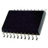
Phase Detectors 3.3V/5V ECL Diff

MC100LVEL40DW

Manufacturer Part Number
MC100LVEL40DW
Description
Phase Detectors 3.3V/5V ECL Diff
Manufacturer
ON Semiconductor
Datasheet

Specifications of MC100LVEL40DW

Package / Case
SOIC-20 Wide
Mounting Style
SMD/SMT
Lead Free Status / RoHS Status
Lead free / RoHS Compliant

Available stocks

Company
Part Number
Manufacturer
Quantity
Price
Part Number:
MC100LVEL40DWR2G
Manufacturer:
ON/安森美
Quantity:
20 000
MC100LVEL40
3.3/5V ECL Differential
Phase−Frequency Detector
Description
intended for phase−locked loop applications which require a minimum
amount of phase and frequency difference at lock. Advanced design
significantly reduces the dead zone of the detector. For proper
operation, the input edge rate of the R and V inputs should be less than
5 ns. The device is designed to work with a 3.3 V power supply.
frequency and/or phase the differential up (U) and down (D) outputs
will provide pulse streams which when subtracted and integrated
provide an error voltage for control of a VCO.
this device only. For single-ended input conditions, the unused
differential input is connected to V
V
and V
to 0.5 mA. When not used, V
Loop Operation.”
Features
*For additional information on our Pb−Free strategy and soldering details, please
© Semiconductor Components Industries, LLC, 2006
November, 2006 − Rev. 8
download the ON Semiconductor Soldering and Mounting Techniques
Reference Manual, SOLDERRM/D.
BB
The MC100LVEL40 is a three state phase frequency−detector
When the reference (R) and the feedback (FB) inputs are unequal in
The V
For application information, refer to AND8040/D, “Phase Lock
The 100 Series Contains Temperature Compensation
250 MHz Typical Bandwidth
PECL Mode Operating Range:
NECL Mode Operating Range:
Internal Input Pulldown Resistor
Pb−Free Packages are Available*
may also rebias AC coupled inputs. When used, decouple V
V
V
CC
CC
CC
BB
via a 0.01 mF capacitor and limit current sourcing or sinking
= 3.0 V to 5.5 V with V
= 0 V with V
pin, an internally generated voltage supply, is available to
EE
= −3.0 V to −5.5 V
BB
should be left open.
BB
EE
as a switching reference voltage.
= 0 V
1
BB
See detailed ordering and shipping information in the package
dimensions section on page 5 of this data sheet.
20
*For additional marking information, refer to
DW SUFFIX
CASE 751D
Application Note AND8002/D.
SO−20
1
ORDERING INFORMATION
A
WL
YY
WW
G
http://onsemi.com
= Assembly Location
= Wafer Lot
= Year
= Work Week
= Pb−Free Package
20
1
Publication Order Number:
AWLYYWWG
100LVEL40
MARKING
DIAGRAM
MC100LVEL40/D

Related parts for MC100LVEL40DW

MC100LVEL40DW Summary of contents

Page 1

... Internal Input Pulldown Resistor • Pb−Free Packages are Available* *For additional information on our Pb−Free strategy and soldering details, please download the ON Semiconductor Soldering and Mounting Techniques Reference Manual, SOLDERRM/D. © Semiconductor Components Industries, LLC, 2006 November, 2006 − Rev. 8 http://onsemi.com ...

Page 2

CCO Warning: All and V pins ...

Page 3

Table 3. MAXIMUM RATINGS Symbol Parameter V PECL Mode Power Supply CC V NECL Mode Power Supply EE V PECL Mode Input Voltage I NECL Mode Input Voltage I Output Current out I V Sink/Source Operating Temperature ...

Page 4

Table 5. LVNECL DC CHARACTERISTICS Symbol Characteristic I Power Supply Current EE V Output HIGH Voltage (Note Output LOW Voltage (Note Input HIGH Voltage IH (Single−Ended) V Input LOW Voltage (Single−Ended Output ...

Page 5

Q Driver Device Q Figure 3. Typical Termination for Output Driver and Device Evaluation (See Application Note AND8020/D − Termination of ECL Logic Devices.) ORDERING INFORMATION Device MC10LVEL40DW MC10LVEL40DWG MC10LVEL40DWR2 MC10LVEL40DWR2G †For information on tape and reel specifications, including part ...

Page 6

... Opportunity/Affirmative Action Employer. This literature is subject to all applicable copyright laws and is not for resale in any manner. PUBLICATION ORDERING INFORMATION LITERATURE FULFILLMENT: Literature Distribution Center for ON Semiconductor P.O. Box 5163, Denver, Colorado 80217 USA Phone: 303−675−2175 or 800−344−3860 Toll Free USA/Canada Fax: 303− ...

Related keywords