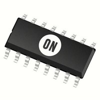
MC14046BDW ON Semiconductor, MC14046BDW Datasheet - Page 6

MC14046BDW
Manufacturer Part Number
MC14046BDW
Description
Phase Locked Loops (PLL) LOG CMOS PLL
Manufacturer
ON Semiconductor
Type
PLLr
Datasheet
1.MC14046BDW.pdf
(8 pages)
Specifications of MC14046BDW
Number Of Circuits
1
Supply Voltage (max)
18 V
Supply Voltage (min)
3 V
Maximum Operating Temperature
+ 125 C
Minimum Operating Temperature
- 55 C
Mounting Style
SMD/SMT
Operating Supply Voltage
3 V to 18 V
Package / Case
SOIC-16 Wide
Lead Free Status / RoHS Status
Lead free / RoHS Compliant
Available stocks
Company
Part Number
Manufacturer
Quantity
Price
Company:
Part Number:
MC14046BDW
Manufacturer:
ON Semiconductor
Quantity:
340
Part Number:
MC14046BDW
Manufacturer:
MOTOROLA/摩托罗拉
Quantity:
20 000
Company:
Part Number:
MC14046BDWG
Manufacturer:
ON
Quantity:
1 398
Part Number:
MC14046BDWR2
Manufacturer:
ON/安森美
Quantity:
20 000
Company:
Part Number:
MC14046BDWR2G
Manufacturer:
ON Semiconductor
Quantity:
500
Part Number:
MC14046BDWR2G
Manufacturer:
ON/安森美
Quantity:
20 000
NOTE: Sometimes R3 is split into two series resistors each R3
Definitions: N = Total division ratio in feedback loop
PC1
VCO
PCA
PCB
@ FREQUENCY f
out
(a)
INPUT
in
in
in
C
the damping, R4 ^ (0.1)(R3) for optimum results.
PCA
C
should be such that the corner frequency of this network does not significantly affect W
in
K VCO +
K = V
K = V
for a typical design W
PCB
Phase Comparator 1
R3
in
C2
DD
DD
14
/ for Phase Comparator 1
/4
2 p D f VCO
3
V DD – 2 V
Note: for further information, see:
(1) F. Gardner, “Phase−Lock Techniques”, John Wiley and Son, New York, 1966.
(2) G. S. Moschytz, “Miniature RC Filters Using Phase−Locked Loop”, BSTJ, May, 1965.
(3) Garth Nash, “Phase−Lock Loop Design Fundamentals”, AN−535, Motorola Inc.
(4) A. B. Przedpelski, “Phase−Locked Loop Design Articles”, AR254, reprinted by Motorola Inc.
for Phase Comparator 2
2f C [ 1 p
Figure 3. General Phase−Locked Loop Connections and Waveforms
OUTPUT
COMPARATOR
PHASE
n
^
^ 0.707
2 p f r
R3 C2
10
2 p f L
2 OR 13
PC1
PC2
OR
(at phase detector input)
out
out
V
V
V
V
V
V
V
V
DD
SS
OH
OL
OH
OL
OH
OL
(a)
INPUT
Typical Low−Pass Filters
EXTERNAL
LOW-PASS
EXTERNAL
COUNTER
FILTER
http://onsemi.com
N
Waveforms
VCO
2. A capacitor C
R3
in
6
9
R4
C2
R1
11
OUTPUT
w n +
z +
F(s) +
9
R2
C
is then placed from the midpoint to ground. The value for
12
FOLLOWER
2K f K VCO
PC2
SOURCE
Filter A
VCO
PCA
PCB
VCO
Nw n
R 3 C 2 S ) 1
LD
out
K f K VCO
6
in
in
in
NR 3 C 2
CI
A
1
CI
Typically:
R 4 C 2 + 6N
(R 3 ) 3, 000W) C 2 + 100NDf
D f = f
LOW−PASS FILTER
10
7
n
CI
Phase Comparator 2
. In Figure B, the ratio of R3 to R4 sets
B
max
4
w n +
z + 0.5 w n (R 3 C 2 )
F(s) +
− f
f max
R
min
SF
S(R 3 C 2 ) R 4 C 2 ) ) 1
SF
–
NC 2 (R 3 ) R 4 )
out
2 p D f
K f K VCO
@ FREQUENCY Nf = f
Filter B
R 3 C 2 S ) 1
N
f max 2
VCO
K f K VCO
out
– R 4 C 2
N
V
V
V
V
V
V
V
V
V
V
)
DD
SS
OH
OL
OH
OL
OH
OL
OH
OL


