DCX54-13 Diodes Inc, DCX54-13 Datasheet
DCX54-13
Specifications of DCX54-13
Available stocks


Related parts for DCX54-13


DCX54-13 Summary of contents
Page 1
... OFF CHARACTERISTICS (Note 4) Collector-Base Breakdown Voltage Collector-Emitter Breakdown Voltage Emitter-Base Breakdown Voltage Collector Cut-off Current Emitter Cut-off Current ON CHARACTERISTICS (Note 4) Collector-Emitter Saturation Voltage Base-Emitter Turn-On Voltage DCX54, DCX54-16 DC Current Gain SMALL SIGNAL CHARACTERISTICS Transition Frequency Output Capacitance Notes purposefully added lead. 2. ...
Page 2
... T , AMBIENT TEMPERATURE (°C) A Fig. 1 Power Dissipation vs. Ambient Temperature (Note 3) DS31229 Rev 125 150 175 www.diodes.com DCX54/-16 © Diodes Incorporated ...
Page 3
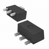
... V , REVERSE VOLTAGE (V) R Fig. 7 Typical Capacitance Characteristics Ordering Information (Note 5) Device DCX54-13 DCX54-16-13 Notes: 5. For packaging details our website at http://www.diodes.com/ap02007.pdf. Marking Information Package Outline Dimensions DS31229 Rev Packaging SOT89-3L SOT89-3L (Top View) = Manufacturer’s code marking ...
Page 4
... Diodes Incorporated products are not authorized for use as critical components in life support devices or systems without the expressed written approval of the President of Diodes Incorporated. DS31229 Rev 2.7 1.9 1.3 Unit: mm IMPORTANT NOTICE LIFE SUPPORT www.diodes.com DCX54/-16 © Diodes Incorporated ...