DXTA42-13 Diodes Inc, DXTA42-13 Datasheet
DXTA42-13
Specifications of DXTA42-13
Available stocks


Related parts for DXTA42-13


DXTA42-13 Summary of contents
Page 1
... I EBO ⎯ ⎯ V CE(SAT) ⎯ ⎯ V BE(SAT) 25 ⎯ ⎯ ⎯ ⎯ C obo www.diodes.com DXTA42 NPN SURFACE MOUNT TRANSISTOR 2 Pin Out Configuration Value Unit 300 V 300 500 mA Value Unit 1 W 125 °C/W -55 to +150 °C Max Unit Test Conditions ⎯ ...
Page 2
... R = 125°C θJA DXTA42 Document number: DS31158 Rev 0.5 0.4 0.3 0.2 0.1 0 0.01 0 COLLECTOR CURRENT (mA) C Fig. 4 Collector-Emitter Saturation Voltage vs. Collector Current www.diodes.com DXTA42 10 100 1,000 December 2009 © Diodes Incorporated ...
Page 3
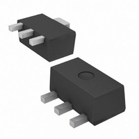
... Ordering Information (Note 5) Part Number DXTA42-13 Notes: 5. For packaging details our website at http://www.diodes.com/datasheets/ap02007.pdf. Marking Information Package Outline Dimensions DXTA42 Document number: DS31158 Rev Case SOT89-3L (Top View) = Manufacturer’s code marking K3M = Product Type Marking Code YWW = Date Code Marking ...
Page 4
... Diodes Incorporated products in such safety-critical, life support devices or systems. Copyright © 2009, Diodes Incorporated www.diodes.com DXTA42 Document number: DS31158 Rev Dimensions Value (in mm IMPORTANT NOTICE LIFE SUPPORT www.diodes.com DXTA42 1.7 0.9 0.4 2.7 1.3 1.9 3.0 December 2009 © Diodes Incorporated ...