MSD602-RT1G ON Semiconductor, MSD602-RT1G Datasheet

TRANS GP NPN 100MA 50V SC59

MSD602-RT1G

Manufacturer Part Number
MSD602-RT1G
Description
TRANS GP NPN 100MA 50V SC59
Manufacturer
ON Semiconductor
Datasheet

Specifications of MSD602-RT1G

Transistor Type
NPN
Current - Collector (ic) (max)
500mA
Voltage - Collector Emitter Breakdown (max)
50V
Vce Saturation (max) @ Ib, Ic
600mV @ 30mA, 300mA
Dc Current Gain (hfe) (min) @ Ic, Vce
120 @ 150mA, 10V
Power - Max
200mW
Mounting Type
Surface Mount
Package / Case
SC-59-3, SMT3, SOT-346, TO-236
Lead Free Status / RoHS Status
Lead free / RoHS Compliant
Current - Collector Cutoff (max)
-
Frequency - Transition
-
Other names
MSD602-RT1GOS

Available stocks

Company
Part Number
Manufacturer
Quantity
Price
Part Number:
MSD602-RT1G
Manufacturer:
ON Semiconductor
Quantity:
500
Part Number:
MSD602-RT1G
Manufacturer:
ON
Quantity:
300 000
Part Number:
MSD602-RT1G
Manufacturer:
ON
Quantity:
12 500
MSD602−RT1
NPN General Purpose
Amplifier Transistor
Surface Mount
Features
Maximum ratings are those values beyond which device damage can occur.
Maximum ratings applied to the device are individual stress limit values (not
normal operating conditions) and are not valid simultaneously. If these limits are
exceeded, device functional operation is not implied, damage may occur and
reliability may be affected.
© Semiconductor Components Industries, LLC, 2006
January, 2006 − Rev. 5
MAXIMUM RATINGS
THERMAL CHARACTERISTICS
Collector−Base Voltage
Collector−Emitter Voltage
Emitter−Base Voltage
Collector Current − Continuous
Collector Current − Peak
Power Dissipation
Junction Temperature
Storage Temperature
Pb−Free Packages are Available
Characteristic
Rating
(T
A
= 25°C)
Preferred Device
V
V
V
Symbol
Symbol
(BR)CBO
(BR)CEO
(BR)EBO
I
T
C(P)
P
T
I
stg
C
D
J
−55 ~ +150
Value
Max
500
200
150
7.0
1.0
60
50
1
mAdc
Unit
Unit
Vdc
Vdc
Vdc
Adc
mW
°C
°C
Preferred devices are recommended choices for future use
and best overall value.
See detailed ordering and shipping information in the package
dimensions section on page 2 of this data sheet.
2
1
3
ORDERING INFORMATION
WR = Specific Device Code
M
G
(Note: Microdot may be in either location)
http://onsemi.com
= Date Code
= Pb−Free Package
BASE
CASE 318D
2
COLLECTOR
SC−59
3
Publication Order Number:
EMITTER
1
MSD602−RT1/D
MARKING
DIAGRAM
WR M G
G

Related parts for MSD602-RT1G

MSD602-RT1G Summary of contents

Page 1

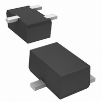
... Pb−Free Package (Note: Microdot may be in either location) ORDERING INFORMATION See detailed ordering and shipping information in the package dimensions section on page 2 of this data sheet. Preferred devices are recommended choices for future use and best overall value. Publication Order Number: MSD602−RT1/D G ...

Page 2

... Pulse Test: Pulse Width ≤ 300 ms, D.C. ≤ 2%. ORDERING INFORMATION Device MSD−602RT1 MSD−602RT1G †For information on tape and reel specifications, including part orientation and tape sizes, please refer to our Tape and Reel Packaging Specifications Brochure, BRD8011/D. MSD602−RT1 (T = 25°C) A Symbol V (BR)CEO ...

Page 3

... Pb−Free strategy and soldering details, please download the ON Semiconductor Soldering and Mounting Techniques Reference Manual, SOLDERRM/D. MSD602−RT1 SC−59 CASE 318D−04 ISSUE G NOTES: 1. DIMENSIONING AND TOLERANCING PER ANSI Y14.5M, 1982. 2. ...

Page 4

... Japan: ON Semiconductor, Japan Customer Focus Center 2−9−1 Kamimeguro, Meguro−ku, Tokyo, Japan 153−0051 Phone: 81−3−5773−3850 http://onsemi.com 4 ON Semiconductor Website: http://onsemi.com Order Literature: http://www.onsemi.com/litorder For additional information, please contact your local Sales Representative. MSD602−RT1/D ...

Related keywords