2N5195G ON Semiconductor, 2N5195G Datasheet

TRANS PNP PWR GP 4A 80V TO225AA

2N5195G

Manufacturer Part Number
2N5195G
Description
TRANS PNP PWR GP 4A 80V TO225AA
Manufacturer
ON Semiconductor
Type
Powerr
Datasheets

Specifications of 2N5195G

Transistor Type
PNP
Current - Collector (ic) (max)
4A
Voltage - Collector Emitter Breakdown (max)
80V
Vce Saturation (max) @ Ib, Ic
1.4V @ 1A, 4A
Current - Collector Cutoff (max)
1mA
Dc Current Gain (hfe) (min) @ Ic, Vce
20 @ 1.5A, 2V
Power - Max
40W
Frequency - Transition
2MHz
Mounting Type
Through Hole
Package / Case
TO-225-3
Transistor Polarity
PNP
Mounting Style
Through Hole
Collector- Emitter Voltage Vceo Max
80 V
Emitter- Base Voltage Vebo
5 V
Maximum Dc Collector Current
4 A
Power Dissipation
40 W
Maximum Operating Temperature
+ 150 C
Continuous Collector Current
4 A
Dc Collector/base Gain Hfe Min
20
Maximum Operating Frequency
2 MHz
Minimum Operating Temperature
- 65 C
Current, Collector
4 A
Current, Gain
7
Frequency
2 MHz
Package Type
TO-225AA
Polarity
PNP
Primary Type
Si
Resistance, Thermal, Junction To Case
3.12 °C/W
Voltage, Breakdown, Collector To Emitter
80 V
Voltage, Collector To Base
80 V
Voltage, Collector To Emitter
80 V
Voltage, Collector To Emitter, Saturation
1.4 V
Voltage, Emitter To Base
5 V
Lead Free Status / RoHS Status
Lead free / RoHS Compliant
Other names
2N5195GOS

Available stocks

Company
Part Number
Manufacturer
Quantity
Price
Part Number:
2N5195G
Manufacturer:
ON
Quantity:
10 000
Company:
Part Number:
2N5195G
Quantity:
2 000
Company:
Part Number:
2N5195G
Quantity:
2 500
Î Î Î Î Î Î Î Î Î Î Î Î Î Î Î Î Î Î Î
Î Î Î Î Î Î Î Î Î Î Î
Î Î Î Î Î Î Î Î Î Î Î Î Î Î Î Î Î Î Î
Î Î Î Î Î Î Î Î Î Î Î
2N5194, 2N5195
Silicon PNP Power
Transistors
circuits; excellent safe area limits. Complement to NPN 2N5191,
2N5192.
Features
Stresses exceeding Maximum Ratings may damage the device. Maximum
Ratings are stress ratings only. Functional operation above the Recommended
Operating Conditions is not implied. Extended exposure to stresses above the
Recommended Operating Conditions may affect device reliability.
1. Indicates JEDEC registered data.
*For additional information on our Pb−Free strategy and soldering details, please
© Semiconductor Components Industries, LLC, 2006
October, 2006 − Rev. 12
MAXIMUM RATINGS
THERMAL CHARACTERISTICS
download the ON Semiconductor Soldering and Mounting Techniques
Reference Manual, SOLDERRM/D.
Collector−Emitter Voltage
Collector−Base Voltage
Emitter−Base Voltage
Collector Current
Base Current
Total Device Dissipation @ T
Derate above 25°C
Operating and Storage Junction
Temperature Range
Thermal Resistance,
Junction−to−Case
These devices are designed for use in power amplifier and switching
Pb−Free Packages are Available*
Characteristic
Rating
(Note 1)
C
Preferred Devices
= 25°C
Î Î Î
Î Î Î
Î Î Î
Î Î Î
Î Î Î
Î Î Î
Î Î Î
Î Î Î
Î Î Î
Î Î Î
Î Î Î
Î Î Î
Î Î Î
Î Î Î
Î Î Î
Î Î Î
Î Î Î
Î Î Î
Î Î Î
Î Î Î
Î Î Î
Î Î Î
Symbol
Symbol
T
V
J
V
V
q
P
, T
CEO
I
I
CB
EB
JC
C
B
D
stg
Î Î Î
Î Î Î
Î Î Î
Î Î Î
Î Î Î
Î Î Î
Î Î Î Î Î Î
Î Î Î Î Î Î
Î Î Î Î Î Î
Î Î Î Î Î Î
Î Î Î Î Î Î
Î Î Î Î Î Î
Î Î Î Î Î Î
Î Î Î Î Î Î
Î Î Î Î Î Î
Î Î Î Î Î Î
Î Î Î Î Î Î
Î Î Î Î Î Î
Î Î Î Î Î Î
Î Î Î Î Î Î
Î Î Î Î Î Î
Î Î Î Î Î Î
2N5194
60
60
– 65 to + 150
Î Î Î Î
Î Î Î Î
Î Î Î Î
Î Î Î Î
Î Î Î Î
Î Î Î Î
Max
3.12
320
5.0
4.0
1.0
40
2N5195
80
80
1
Î Î Î Î
Î Î
Î Î
Î Î
Î Î
Î Î
Î Î
Î Î
Î Î
Î Î Î Î
Î Î
Î Î
Î Î
Î Î
Î Î
Î Î
Î Î
Î Î
Î Î
Î Î
W/°C
°C/W
°C/W
Unit
Unit
Vdc
Vdc
Vdc
Adc
Adc
W
Preferred devices are recommended choices for future use
and best overall value.
2N5194
2N5194G
2N5195
2N5195G
Device
POWER TRANSISTORS
ORDERING INFORMATION
Y
WW
2N519x = Device Code
G
MARKING DIAGRAM
60 − 80 VOLTS
http://onsemi.com
PNP SILICON
4 AMPERE
(Pb−Free)
(Pb−Free)
Package
TO−225
TO−225
TO−225
TO−225
= Year
= Work Week
= Pb−Free Package
YWW
2
N519xG
x = 4 or 5
Publication Order Number:
CASE 77−09
TO−225AA
STYLE 1
500 Units / Bulk
500 Units / Bulk
500 Units / Bulk
500 Units / Bulk
Shipping
2N5194/D

Related parts for 2N5195G

2N5195G Summary of contents

Page 1

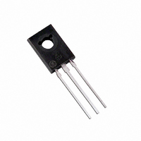
... Shipping Device Package 2N5194 TO−225 500 Units / Bulk 2N5194G TO−225 500 Units / Bulk (Pb−Free) 2N5195 TO−225 500 Units / Bulk 2N5195G TO−225 500 Units / Bulk (Pb−Free) Preferred devices are recommended choices for future use and best overall value. Publication Order Number: 2N5194/D ...

Page 2

ELECTRICAL CHARACTERISTICS Î Î Î Î Î ...

Page 3

100 25°C J 0.4 0 0.05 0.07 0.1 0.2 0.3 0.5 0.7 1.0 2 25°C J 1.6 1.2 0 BE(sat) ...

Page 4

V CC TURN−ON PULSE V BE(off APPROX C << C − APPROX +9 APPROX ≤ 7 − < 500 ms ...

Page 5

D = 0.5 0.5 0.3 0.2 0.2 0.1 0.1 0.05 0.07 0.02 0.05 0.01 0.03 SINGLE PULSE 0.02 0.01 0.01 0.02 0.03 0.05 0.1 0.2 0.3 DESIGN NOTE: USE OF TRANSIENT THERMAL RESISTANCE DATA ...

Page 6

... Opportunity/Affirmative Action Employer. This literature is subject to all applicable copyright laws and is not for resale in any manner. PUBLICATION ORDERING INFORMATION LITERATURE FULFILLMENT: Literature Distribution Center for ON Semiconductor P.O. Box 5163, Denver, Colorado 80217 USA Phone: 303−675−2175 or 800−344−3860 Toll Free USA/Canada Fax: 303− ...

Related keywords