Î Î Î Î Î Î Î Î Î Î Î Î Î Î Î Î Î Î Î Î
Î Î Î Î Î Î Î Î Î Î Î Î Î Î Î Î Î Î Î Î
Î Î Î Î Î Î Î Î Î Î Î Î Î
Î Î Î Î Î Î Î Î Î Î Î Î Î
Î Î Î Î Î Î Î Î Î Î Î Î Î
Î Î Î Î Î Î Î Î Î Î Î Î Î
Î Î Î Î Î Î Î Î Î Î Î Î Î
Î Î Î Î Î Î Î Î Î Î Î Î Î
Î Î Î Î Î Î Î Î Î Î Î Î Î
Î Î Î Î Î Î Î Î Î Î Î Î Î
Î Î Î Î Î Î Î Î Î Î Î Î Î
Î Î Î Î Î Î Î Î Î Î Î Î Î
Î Î Î Î Î Î Î Î Î Î Î Î Î
Î Î Î Î Î Î Î Î Î Î Î Î Î
Î Î Î Î Î Î Î Î Î Î Î Î Î
Î Î Î Î Î Î Î Î Î Î Î Î Î
Î Î Î Î Î Î Î Î Î Î Î Î Î
Î Î Î Î Î Î Î Î Î Î Î Î Î
Î Î Î Î Î Î Î Î Î Î Î Î Î
Î Î Î Î Î Î Î Î Î Î Î Î Î
Î Î Î Î Î Î Î Î Î Î Î Î Î
Î Î Î Î Î Î Î Î Î Î Î Î Î
Î Î Î Î Î Î Î Î Î Î Î Î Î
Î Î Î Î Î Î Î Î Î Î Î Î Î Î Î Î Î Î Î Î
Î Î Î Î Î Î Î Î Î Î Î Î Î Î Î Î Î Î Î Î
Î Î Î Î Î Î Î Î Î Î Î Î Î
Î Î Î Î Î Î Î Î Î Î Î Î Î
Î Î Î Î Î Î Î Î Î Î Î Î Î
Î Î Î Î Î Î Î Î Î Î Î Î Î
Î Î Î Î Î Î Î Î Î Î Î Î Î
Î Î Î Î Î Î Î Î Î Î Î Î Î
Î Î Î Î Î Î Î Î Î Î Î Î Î
Î Î Î Î Î Î Î Î Î Î Î Î Î
MJF3055 (NPN),
MJF2955 (PNP)
Complementary
Silicon Power Transistors
applications.
Features
•
•
•
•
•
•
•
•
•
•
Maximum ratings are those values beyond which device damage can occur.
Maximum ratings applied to the device are individual stress limit values (not
normal operating conditions) and are not valid simultaneously. If these limits are
exceeded, device functional operation is not implied, damage may occur and
reliability may be affected.
1. Pulse Test: Pulse Width = 5.0 ms, Duty Cycle v 10%.
2. Measurement made with thermocouple contacting the bottom insulated
3. Proper strike and creepage distance must be provided.
*For additional information on our Pb−Free strategy and soldering details,
© Semiconductor Components Industries, LLC, 2008
July, 2008 − Rev. 7
MAXIMUM RATINGS
THERMAL CHARACTERISTICS
please download the ON Semiconductor Soldering and Mounting Techniques
Reference Manual, SOLDERRM/D.
Collector−Emitter Sustaining Voltage
Collector−Emitter Breakdown Voltage
Base−Emitter Voltage
Collector Current − Continuous
Base Current − Continuous
RMS Isolation Voltage (Note 3)
Total Power Dissipation @ T
Total Power Dissipation @ T
Operating and Storage Temperature Range
Thermal Resistance, Junction−to−Case (Note 2)
Thermal Resistance, Junction−to−Ambient
Lead Temperature for Soldering Purposes
Specifically designed for general purpose amplifier and switching
Isolated Overmold Package (1500 Volts RMS Min)
Electrically Similar to the Popular MJE3055T and MJE2955T
Collector−Emitter Sustaining Voltage − V
10 Amperes Rated Collector Current
No Isolating Washers Required
Reduced System Cost
UL Recognized, File #E69369, to 3500 V
Epoxy Meets UL 94 V−0 at 0.125 in
ESD Ratings: Machine Model, C; u400 V
Pb−Free Packages are Available*
surface (in a location beneath the die), the devices mounted on a heatsink with
thermal grease and a mounting torque of ≥ 6 in. lbs.
(t = 0.3 sec, R.H. ≤ 30%, T
Per Figure 5
Derate above 25_C
Derate above 25_C
Characteristic
Human Body Model, 3B; u8000 V
Rating
C
A
A
= 25_C
= 25_C (Note 2)
= 25_C)
Î Î Î Î
Î Î Î Î
Î Î Î Î
Î Î Î Î
Î Î Î Î
Î Î Î Î
Î Î Î Î
Î Î Î Î
Î Î Î Î
Î Î Î Î
Î Î Î Î
Î Î Î Î
Î Î Î Î
Î Î Î Î
Î Î Î Î
Î Î Î Î
Î Î Î Î
Î Î Î Î
Î Î Î Î
Î Î Î Î
Î Î Î Î
Î Î Î Î
Î Î Î Î
Î Î Î Î
Î Î Î Î
Î Î Î Î
Î Î Î Î
Î Î Î Î
Î Î Î Î
CEO(sus)
RMS
V
Symbol
Symbol
T
CEO(sus)
V
V
V
R
R
J
P
P
EBO
ISOL
, T
T
CES
I
I
qJC
qJA
C
B
Isolation
D
D
L
stg
90 Volts
Î Î Î
Î Î Î
Î Î Î
Î Î Î
Î Î Î
Î Î Î
Î Î Î
Î Î Î
Î Î Î
Î Î Î
Î Î Î
Î Î Î
Î Î Î
Î Î Î
Î Î Î
Î Î Î
Î Î Î
Î Î Î
Î Î Î
Î Î Î
Î Î Î
Î Î Î
Î Î Î
Î Î Î
Î Î Î
Î Î Î
Î Î Î
Î Î Î
Î Î Î
Value
–55 to
0.016
4500
+150
0.25
Max
62.5
260
5.0
6.0
2.0
4.0
90
90
10
30
1
Î Î Î
Î Î Î
Î Î Î
Î Î Î
Î Î Î
Î Î Î
Î Î Î
Î Î Î
Î Î Î
Î Î Î
Î Î Î
Î Î Î
Î Î Î
Î Î Î
Î Î Î
Î Î Î
Î Î Î
Î Î Î
Î Î Î
Î Î Î
Î Î Î
Î Î Î
Î Î Î
Î Î Î
Î Î Î
Î Î Î
Î Î Î
Î Î Î
Î Î Î
V
W/_C
W/_C
_C/W
_C/W
Unit
Unit
Vdc
Vdc
Vdc
Adc
Adc
_C
_C
RMS
W
W
MJF2955
MJF2955G
MJF3055
MJF3055G
Device
COMPLEMENTARY SILICON
1
POWER TRANSISTORS
2
90 VOLTS, 30 WATTS
Fxx55 = Specific Device Code
G
A
Y
WW
ORDERING INFORMATION
3
MARKING DIAGRAM
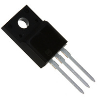
TO−220 FULLPACK
TO−220 FULLPACK
http://onsemi.com
TO−220 FULLPACK
10 AMPERES
TO−220 FULLPACK
= Pb−Free Package
= Assembly Location
= Year
= Work Week
xx= 29 or 30
(Pb−Free)
(Pb−Free)
Package
Fxx55G
TO−220 FULLPACK
AYWW
Publication Order Number:
CASE 221D
STYLE 2
50 Units/Rail
50 Units/Rail
50 Units/Rail
50 Units/Rail
Shipping
MJF3055/D