MJW18020G ON Semiconductor, MJW18020G Datasheet

TRANS PWR NPN 20A 450V TO-247

MJW18020G

Manufacturer Part Number
MJW18020G
Description
TRANS PWR NPN 20A 450V TO-247
Manufacturer
ON Semiconductor
Datasheet

Specifications of MJW18020G

Transistor Type
NPN
Current - Collector (ic) (max)
30A
Voltage - Collector Emitter Breakdown (max)
450V
Vce Saturation (max) @ Ib, Ic
1.5V @ 4A, 20A
Current - Collector Cutoff (max)
100µA
Dc Current Gain (hfe) (min) @ Ic, Vce
14 @ 3A, 5V
Power - Max
250W
Frequency - Transition
13MHz
Mounting Type
Through Hole
Package / Case
TO-247-3 (Straight Leads), TO-247AC
Transistor Polarity
NPN
Mounting Style
SMD/SMT
Collector- Emitter Voltage Vceo Max
1000 V
Emitter- Base Voltage Vebo
9 V
Maximum Dc Collector Current
30 A
Power Dissipation
250 W
Maximum Operating Temperature
+ 150 C
Continuous Collector Current
30 A
Dc Collector/base Gain Hfe Min
14
Maximum Operating Frequency
13 MHz
Minimum Operating Temperature
- 65 C
Lead Free Status / RoHS Status
Lead free / RoHS Compliant

Available stocks

Company
Part Number
Manufacturer
Quantity
Price
Part Number:
MJW18020G
Manufacturer:
OMRON
Quantity:
5 523
Part Number:
MJW18020G
Manufacturer:
ON/安森美
Quantity:
20 000
MJW18020
NPN Silicon Power
Transistors High Voltage
Planar
specifically Designed for motor control applications, high power
supplies and UPS’s for which the high reproducibility of DC and
Switching parameters minimizes the dead time in bridge
configurations.
Features
Stresses exceeding Maximum Ratings may damage the device. Maximum
Ratings are stress ratings only. Functional operation above the Recommended
Operating Conditions is not implied. Extended exposure to stresses above the
Recommended Operating Conditions may affect device reliability.
1. Pulse Test: Pulse Width = 5 ms, Duty Cycle ≤ 10%.
*For additional information on our Pb−Free strategy and soldering details, please
© Semiconductor Components Industries, LLC, 2010
March, 2010 − Rev. 2
MAXIMUM RATINGS
THERMAL CHARACTERISTICS
download the ON Semiconductor Soldering and Mounting Techniques
Reference Manual, SOLDERRM/D.
Collector−Emitter Sustaining Voltage
Collector−Base Breakdown Voltage
Collector−Base Voltage
Emitter−Base Voltage
Collector Current − Continuous
Base Current
Total Power Dissipation @ T
Derate Above 25_C
Operating and Storage Junction
Temperature Range
Thermal Resistance, Junction−to−Case
Thermal Resistance, Junction−to−Ambient
Maximum Lead Temperature for Soldering
Purposes: 1/8” from Case for 5 Seconds
The MJW18020 planar High Voltage Power Transistor is
High and Excellent Gain Linearity
Fast and Very Tight Switching Times Parameters t
Very Stable Leakage Current due to the Planar Structure
High Reliability
Pb−Free Package is Available*
Characteristic
Rating
− Peak (Note 1)
− Continuous
− Peak (Note 1)
C
= 25_C
Symbol
Symbol
T
V
V
V
V
R
R
J
P
CEO
CBO
EBO
, T
T
CES
I
I
qJC
qJA
C
B
D
L
stg
−65 to +150
si
Value
1000
1000
Max
450
250
275
9.0
6.0
2.0
0.5
and t
30
45
10
50
fi
1
W/_C
_C/W
_C/W
Unit
Unit
Vdc
Vdc
Vdc
Vdc
Adc
Adc
_C
_C
W
MJW18020
MJW18020G
450 VOLTS BV
Device
1
ORDERING INFORMATION
2
1 BASE
1000 VOLTS BV
A
Y
WW
G
3
MARKING DIAGRAM
http://onsemi.com
30 AMPERES
2 COLLECTOR
= Assembly Location
= Year
= Work Week
= Pb−Free Package
(Pb−Free)
Package
MJW18020
TO−247
TO−247
AYWWG
CEO,
Publication Order Number:
CASE 340L
250 WATTS
3 EMITTER
TO−247
CES
30 Units/Rail
30 Units/Rail
Shipping
MJW18020/D

Related parts for MJW18020G

MJW18020G Summary of contents

Page 1

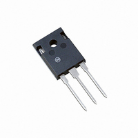
... W/ −65 to +150 _C J stg Symbol Max Unit R 0.5 _C/W qJC R 50 _C/W qJA T 275 _C L MJW18020 MJW18020G 1 http://onsemi.com 30 AMPERES 1000 VOLTS BV CES 250 WATTS CEO TO−247 3 CASE 340L MARKING DIAGRAM MJW18020 AYWWG 1 BASE 3 EMITTER 2 COLLECTOR A = Assembly Location Y = Year WW = Work Week G = Pb− ...

Page 2

ELECTRICAL CHARACTERISTICS (T Characteristic OFF CHARACTERISTICS Collector−Emitter Sustaining Voltage (I = 100 mAdc Collector Cutoff Current (V = Rated CEO B Collector Cutoff Current (V = Rated V CE ...

Page 3

T = 125° −20° 2 1.0 0.01 0.1 1 COLLECTOR CURRENT (A) C Figure 1. DC Current Gain, V 100 5 10.0 1.0 ...

Page 4

C ib 1000 C ob 100 COLLECTOR−EMITTER VOLTAGE (VOLTS) CE Figure 7. Typical Capacitance Figure 9. Reverse Bias Safe Operating Area TYPICAL CHARACTERISTICS 100.00 DC 10.00 1.00 0.10 ...

Page 5

... Opportunity/Affirmative Action Employer. This literature is subject to all applicable copyright laws and is not for resale in any manner. PUBLICATION ORDERING INFORMATION LITERATURE FULFILLMENT: Literature Distribution Center for ON Semiconductor P.O. Box 5163, Denver, Colorado 80217 USA Phone: 303−675−2175 or 800−344−3860 Toll Free USA/Canada Fax: 303− ...

Related keywords