BUV22G ON Semiconductor, BUV22G Datasheet - Page 3
BUV22G
Manufacturer Part Number
BUV22G
Description
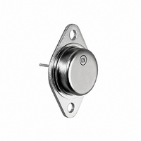
TRANS NPN 250V 40A BIPO TO-3
Manufacturer
ON Semiconductor
Series
SWITCHMODE™r
Datasheet
1.BUV22G.pdf
(4 pages)
Specifications of BUV22G
Transistor Type
NPN
Current - Collector (ic) (max)
40A
Voltage - Collector Emitter Breakdown (max)
250V
Vce Saturation (max) @ Ib, Ic
1.5V @ 2.5A, 20A
Current - Collector Cutoff (max)
3mA
Dc Current Gain (hfe) (min) @ Ic, Vce
20 @ 10A, 4V
Power - Max
250W
Frequency - Transition
8MHz
Mounting Type
Chassis Mount
Package / Case
TO-204, TO-3
Lead Free Status / RoHS Status
Lead free / RoHS Compliant


0.1
40
10
1
2.0
1.6
1.2
0.8
0.4
3.0
2.0
1.0
0.4
0.3
0.2
1
0
4
Figure 2. Active Region Safe Operating Area
Figure 5. Resistive Switching Performance
V
CE
8
, COLLECTOR−EMITTER VOLTAGE (V)
Figure 3. “On” Voltages
I
I
C
C
10
, COLLECTOR CURRENT (A)
, COLLECTOR CURRENT (A)
1
12
I
C
/I
B
= 8
16
100
10
V
V
BE
CE
250
20
t
t
t
on
F
S
http://onsemi.com
BUV22
24
3
a transistor: average junction temperature and second
breakdown. Safe operating area curves indicate I
limits of the transistor that must be observed for reliable
operation i.e., the transistor must not be subjected to greater
dissipation than the curves indicate.
variable depending on power level. Second breakdown
limitations do not derate the same as thermal limitations.
the power that can handled to values less than the limitations
imposed by second breakdown.
50
45
40
35
30
25
20
15
10
There are two limitations on the power handling ability of
The data of Figure 2 is based on T
At high case temperatures, thermal limitations will reduce
5
0
0.1
R
C
Figure 6. Switching Times Test Circuit
− R
B
I
B1
: Non inductive resistances
Figure 4. DC Current Gain
I
I
C
B2
, COLLECTOR CURRENT (A)
1
R
B
R
C
V
CC
10
C
= 25_C; T
10
I
V
V
C
R
R
I
CC
/I
CE
B1
4
C
B
B
mF
= 5 V
= 100 V
= 5 W
= 2.7 W
= I
= 8
B2
C
J(pk)
− V
100
CE
is
Related parts for BUV22G
Image
Part Number
Description
Manufacturer
Datasheet
Request
R

Part Number:
Description:
TRANS NPN 250V 40A BIPO TO-3
Manufacturer:
ON Semiconductor
Datasheet:

Part Number:
Description:
ON Semiconductor [VOLTAGE REGULATOR]
Manufacturer:
ON Semiconductor
Datasheet:
Part Number:
Description:
357-036-542-201 CARDEDGE 36POS DL .156 BLK LOPRO
Manufacturer:
ON Semiconductor
Datasheet:
Part Number:
Description:
357-036-542-201 CARDEDGE 36POS DL .156 BLK LOPRO
Manufacturer:
ON Semiconductor
Datasheet:
Part Number:
Description:
357-036-542-201 CARDEDGE 36POS DL .156 BLK LOPRO
Manufacturer:
ON Semiconductor
Datasheet:
Part Number:
Description:
357-036-542-201 CARDEDGE 36POS DL .156 BLK LOPRO
Manufacturer:
ON Semiconductor
Datasheet:
Part Number:
Description:
357-036-542-201 CARDEDGE 36POS DL .156 BLK LOPRO
Manufacturer:
ON Semiconductor
Datasheet:
Part Number:
Description:
357-036-542-201 CARDEDGE 36POS DL .156 BLK LOPRO
Manufacturer:
ON Semiconductor
Datasheet:
Part Number:
Description:
357-036-542-201 CARDEDGE 36POS DL .156 BLK LOPRO
Manufacturer:
ON Semiconductor
Datasheet:
Part Number:
Description:
357-036-542-201 CARDEDGE 36POS DL .156 BLK LOPRO
Manufacturer:
ON Semiconductor
Datasheet:
Part Number:
Description:
357-036-542-201 CARDEDGE 36POS DL .156 BLK LOPRO
Manufacturer:
ON Semiconductor
Datasheet:
Part Number:
Description:
357-036-542-201 CARDEDGE 36POS DL .156 BLK LOPRO
Manufacturer:
ON Semiconductor
Datasheet:
Part Number:
Description:
Manufacturer:
ON Semiconductor
Datasheet:
Part Number:
Description:
Manufacturer:
ON Semiconductor
Datasheet: