2N4923 ON Semiconductor, 2N4923 Datasheet

TRANS NPN GP 1A 80V HP TO225AA

2N4923

Manufacturer Part Number
2N4923
Description
TRANS NPN GP 1A 80V HP TO225AA
Manufacturer
ON Semiconductor
Datasheet

Specifications of 2N4923

Transistor Type
NPN
Current - Collector (ic) (max)
1A
Voltage - Collector Emitter Breakdown (max)
80V
Vce Saturation (max) @ Ib, Ic
600mV @ 100mA, 1A
Dc Current Gain (hfe) (min) @ Ic, Vce
30 @ 500mA, 1V
Power - Max
30W
Frequency - Transition
3MHz
Mounting Type
Through Hole
Package / Case
TO-225-3
Lead Free Status / RoHS Status
Contains lead / RoHS non-compliant
Current - Collector Cutoff (max)
-
Other names
2N4923OS

Available stocks

Company
Part Number
Manufacturer
Quantity
Price
Part Number:
2N4923
Manufacturer:
ST
0
Company:
Part Number:
2N4923
Quantity:
100
Part Number:
2N4923G
Manufacturer:
ON Semiconductor
Quantity:
5 150
Part Number:
2N4923G
Manufacturer:
ON/安森美
Quantity:
20 000
Î Î Î Î Î Î Î Î Î Î Î Î
2N4921, 2N4922, 2N4923
Medium−Power Plastic
NPN Silicon Transistors
circuits, switching, and amplifier applications.
Features
Maximum ratings are those values beyond which device damage can occur.
Maximum ratings applied to the device are individual stress limit values (not
normal operating conditions) and are not valid simultaneously. If these limits are
exceeded, device functional operation is not implied, damage may occur and
reliability may be affected.
1. The 1.0 A maximum I
2. Recommend use of thermal compound for lowest thermal resistance.
*Indicates JEDEC Registered Data.
*For additional information on our Pb−Free strategy and soldering details, please
© Semiconductor Components Industries, LLC, 2006
January, 2006 − Rev. 11
MAXIMUM RATINGS
THERMAL CHARACTERISTICS
Collector−Emitter Voltage
Emitter Base Voltage
Collector Current − Continuous (Note 1)
Base Current
Total Power Dissipation @ T
Operating and Storage Junction
Temperature Range
Thermal Resistance, Junction−to−Case
download the ON Semiconductor Soldering and Mounting Techniques
Reference Manual, SOLDERRM/D.
These high−performance plastic devices are designed for driver
Low Saturation Voltage − V
Excellent Power Dissipation Due to Thermopad Construction −
Excellent Safe Operating Area
Gain Specified to I
Complement to PNP 2N4918, 2N4919, 2N4920
Pb−Free Packages are Available*
The 3.0 A maximum value is based upon actual current handling capability of
the device (see Figures 5 and 6).
Derate above 25_C
P
D
= 30 W @ T
Characteristic
Rating
− Continuous
C
C
C
2N4923 is a Preferred Device
value is based upon JEDEC current gain requirements.
= 1.0 A
= 25_C
C
= 25_C
CE(sat)
2N4921
2N4922
2N4923
2N4921
2N4922
2N4923
(Note 2)
= 0.6 Vdc (Max) @ I
Î Î Î
Î Î Î
Î Î Î
Î Î Î
Î Î Î
Î Î Î
Î Î Î
Î Î Î
Î Î Î
Î Î Î
Î Î Î
Î Î Î
Î Î Î
Î Î Î
Î Î Î
Î Î Î
Î Î Î
Î Î Î
Î Î Î
Î Î Î
Symbol
Symbol
T
V
J
V
V
q
P
, T
CEO
I
I
CB
EB
JC
C
B
D
stg
Î Î Î Î
Î Î Î Î
Î Î Î Î
Î Î Î Î
Î Î Î Î
Î Î Î Î
Î Î Î Î
Î Î Î Î
Î Î Î Î
Î Î Î Î
Î Î Î Î
Î Î Î Î
Î Î Î Î
Î Î Î Î
Î Î Î Î
Î Î Î Î
Î Î Î Î
Î Î Î Î
Î Î Î Î
Î Î Î Î
–65 to +150
Value
0.24
Max
4.16
5.0
1.0
3.0
1.0
40
60
80
40
60
80
30
Î Î Î Î
Î Î Î Î
Î Î Î Î
Î Î Î Î
Î Î Î Î
Î Î Î Î
Î Î Î Î
Î Î Î Î
Î Î Î Î
Î Î Î Î
Î Î Î Î
Î Î Î Î
Î Î Î Î
Î Î Î Î
Î Î Î Î
Î Î Î Î
Î Î Î Î
Î Î Î Î
Î Î Î Î
Î Î Î Î
C
= 1.0 A
1
mW/_C
_C/W
Unit
Unit
Vdc
Vdc
Vdc
Adc
Adc
_C
W
Preferred devices are recommended choices for future use
and best overall value.
2N4921
2N4921G
2N4922
2N4922G
2N4923
2N4923G
Device
40−80 VOLTS, 30 WATTS
POWER TRANSISTORS
3
GENERAL PURPOSE
ORDERING INFORMATION
Y
WW
2N492x = Device Code
G
2 1
MARKING DIAGRAM
1
http://onsemi.com
1.0 AMPERE
(Pb−Free)
(Pb−Free)
(Pb−Free)
Package
TO−225
TO−225
TO−225
TO−225
TO−225
TO−225
= Year
= Work Week
= Pb−Free Package
x = 1, 2, or 3
N492xG
YWW
Publication Order Number:
2
CASE 77
STYLE 1
TO−225
500 Units / Box
500 Units / Box
500 Units / Box
500 Units / Box
500 Units / Box
500 Units / Box
Shipping
2N4921/D

Related parts for 2N4923

2N4923 Summary of contents

Page 1

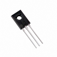
... Preferred Device Medium−Power Plastic NPN Silicon Transistors These high−performance plastic devices are designed for driver circuits, switching, and amplifier applications. Features • Low Saturation Voltage − V CE(sat) • Excellent Power Dissipation Due to Thermopad Construction − ...

Page 2

... CE 3. Pulse Test: PW ≈ 300 ms, Duty Cycle ≈ 2.0%. Î Î Î Î Î Î Î Î Î Î Î Î Î Î Î Î Î Î Î Î Î *Indicates JEDEC Registered Data. 2N4921, 2N4922, 2N4923 (T = 25_C unless otherwise noted) C Î ...

Page 3

... T , CASE TEMPERATURE (°C) C Figure 1. Power Derating Safe Area Curves are indicated by Figure 5. All limits are applicable and must be observed. APPROX TURN−ON PULSE + BE(off APPROX SCOPE + APPROX 9 TURN−OFF PULSE Figure 2. Switching Time Equivalent Circuit 5 3 2.0 1.0 ...

Page 4

... 0 ′ − 1 100 200 300 I , COLLECTOR CURRENT (mA) C Figure 6. Storage Time 2N4921, 2N4922, 2N4923 q ( 4.16°C/W MAX JC D CURVES APPLY FOR POWER PULSE TRAIN SHOWN READ TIME − J(pk) C (pk) 0.5 1.0 2.0 3.0 5 TIME (ms) Figure 4 ...

Page 5

... CES 0 10 −1 10 REVERSE FORWARD − −0.2 −0.1 0 +0.1 +0 BASE−EMITTER VOLTAGE (VOLTS) BE Figure 12. Collector Cut−Off Region 2N4921, 2N4922, 2N4923 0.8 0.6 0.4 0.2 0 1000 2000 0.2 0.3 0.5 Figure 9. Collector Saturation Region 1 25° 1.2 0.9 ...

Page 6

... Literature Distribution Center for ON Semiconductor P.O. Box 61312, Phoenix, Arizona 85082−1312 USA Phone: 480−829−7710 or 800−344−3860 Toll Free USA/Canada Fax: 480−829−7709 or 800−344−3867 Toll Free USA/Canada Email: orderlit@onsemi.com 2N4921, 2N4922, 2N4923 PACKAGE DIMENSIONS TO−225 CASE 77−09 ISSUE Z ...

Related keywords