2N6488 ON Semiconductor, 2N6488 Datasheet
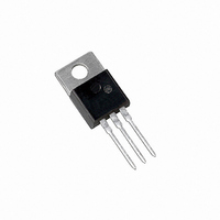
TRANS PWR NPN 15A 80V TO220AB

2N6488

Manufacturer Part Number
2N6488
Description
TRANS PWR NPN 15A 80V TO220AB
Manufacturer
ON Semiconductor
Datasheet

Specifications of 2N6488

Transistor Type
NPN
Current - Collector (ic) (max)
15A
Voltage - Collector Emitter Breakdown (max)
80V
Vce Saturation (max) @ Ib, Ic
3.5V @ 5A, 15A
Current - Collector Cutoff (max)
1mA
Dc Current Gain (hfe) (min) @ Ic, Vce
20 @ 5A, 4V
Power - Max
1.8W
Frequency - Transition
5MHz
Mounting Type
Through Hole
Package / Case
TO-220-3 (Straight Leads)
Lead Free Status / RoHS Status
Contains lead / RoHS non-compliant
Other names
2N6488OS

Available stocks

Company
Part Number
Manufacturer
Quantity
Price
Part Number:
2N6488
Manufacturer:
ON
Quantity:
5 000
Part Number:
2N6488
Manufacturer:
INFINEON
Quantity:
47
Part Number:
2N6488
Manufacturer:
ST
0
Part Number:
2N6488
Manufacturer:
ON/安森美
Quantity:
20 000
Part Number:
2N6488G
Manufacturer:
ON
Quantity:
970
Part Number:
2N6488G
Manufacturer:
ON Semiconductor
Quantity:
10
Part Number:
2N6488G
Manufacturer:
ON/安森美
Quantity:
20 000
2N6487, 2N6488, (NPN)
2N6490, 2N6491 (PNP)
Complementary Silicon
Plastic Power Transistors
switching applications.
Features
Stresses exceeding Maximum Ratings may damage the device. Maximum
Ratings are stress ratings only. Functional operation above the Recommended
Operating Conditions is not implied. Extended exposure to stresses above the
Recommended Operating Conditions may affect device reliability.
1. Indicates JEDEC Registered Data.
*For additional information on our Pb-Free strategy and soldering details, please
MAXIMUM RATINGS
THERMAL CHARACTERISTICS
© Semiconductor Components Industries, LLC, 2007
November, 2007 - Rev. 13
download the ON Semiconductor Soldering and Mounting Techniques
Reference Manual, SOLDERRM/D.
Collector-Emitter Voltage
Collector-Base Voltage
Emitter-Base Voltage
Collector Current - Continuous
Base Current
Total Power Dissipation @ T
Derate above 25_C
Total Power Dissipation @ T
Derate above 25_C
Operating and Storage Junction
Temperature Range
Thermal Resistance, Junction-to-Case
Thermal Resistance, Junction-to-Ambient
These devices are designed for use in general-purpose amplifier and
DC Current Gain Specified to 15 Amperes -
Collector-Emitter Sustaining Voltage -
High Current Gain - Bandwidth Product
TO-220AB Compact Package
Pb-Free Packages are Available*
h
V
f
T
FE
Characteristics
CEO(sus)
= 5.0 MHz (Min) @ I
2N6488 and 2N6491 are Preferred Devices
= 20-150 @ I
= 5.0 (Min) @ I
Rating
(Note 1)
= 60 Vdc (Min) - 2N6487, 2N6490
= 80 Vdc (Min) - 2N6488, 2N6491
2N6487, 2N6490
2N6488, 2N6491
2N6487, 2N6490
2N6488, 2N6491
A
C
= 25_C
= 25_C
C
C
= 5.0 Adc
= 15 Adc
C
= 1.0 Adc
Symbol
Symbol
T
V
R
R
J
V
V
P
P
CEO
, T
I
I
qJC
qJA
CB
EB
C
B
D
D
stg
-65 to +150
Value
0.014
Max
1.67
5.0
5.0
0.6
1.8
60
80
70
90
15
75
70
1
_C/W
_C/W
W/°C
W/°C
Unit
Vdc
Vdc
Vdc
Adc
Adc
Unit
°C
W
W
See detailed ordering, marking, and shipping information in
the package dimensions section on page 5 of this data sheet.
Preferred devices are recommended choices for future use
and best overall value.
1
2
COMPLEMENTARY SILICON
3
60-80 VOLTS, 75 WATTS
POWER TRANSISTORS
2N64xx = Specific Device Code
xx
G
A
Y
WW
ORDERING INFORMATION
http://onsemi.com
4
15 AMPERE
CASE 221A
= See Table on Page 5
= Pb-Free Package
= Assembly Location
= Year
= Work Week
TO-220AB
STYLE 1
Publication Order Number:
MARKING
DIAGRAM
2N64xxG
AYWW
2N6487/D

Related parts for 2N6488

2N6488 Summary of contents

Page 1

... I = 5.0 Adc 5.0 (Min Adc C • Collector-Emitter Sustaining Voltage - Vdc (Min) - 2N6487, 2N6490 CEO(sus Vdc (Min) - 2N6488, 2N6491 • High Current Gain - Bandwidth Product f = 5.0 MHz (Min • TO-220AB Compact Package • Pb-Free Packages are Available* MAXIMUM RATINGS (Note 1) Rating ...

Page 2

... T 4.0 3.0 2.0 1.0 Î Î Î Î Î Î Î Î Î Î Î Î Î Î Î Î Î Î Î Î Î Î Î Î Î Î Î Î Î Î Î Î Î ...

Page 3

... DUTY CYCLE = 1.0% R AND R B FOR PNP, REVERSE ALL POLARITIES. D MUST BE FAST RECOVERY TYPE, e.g.: 1 1N5825 USED ABOVE I MSD6100 USED BELOW I 1000 500 200 100 25° 0.2 1.0 0 0.5 0.5 0.3 0.2 0.2 0.1 0.1 ...

Page 4

... T = 150°C J 1.0 SECOND BREAKDOWN LIMITED BONDING WIRE LIMITED 0.5 THERMALLY LIMITED @ T = 25°C C CURVES APPLY BELOW RATED V CEO 0.2 2N6487, 2N6490 2N6488, 2N6491 0.1 2.0 4 COLLECTOR-EMITTER VOLTAGE (VOLTS) CE Figure 5. Active-Region Safe Operating Area ...

Page 5

... 1.0 0.8 4.0 A 0.6 0.4 0 100 200 I , BASE CURRENT (mA 25°C 2.4 J 2.0 1.6 1 BE(sat CE(sat 0.2 0.5 1.0 2 COLLECTOR CURRENT (AMP) C ORDERING INFORMATION Device 2N6487 ...

Page 6

... Semiconductor and are registered trademarks of Semiconductor Components Industries, LLC (SCILLC). SCILLC reserves the right to make changes without further notice to any products herein. SCILLC makes no warranty, representation or guarantee regarding the suitability of its products for any particular purpose, nor does SCILLC assume any liability arising out of the application or use of any product or circuit, and specifically disclaims any and all liability, including without limitation special, consequential or incidental damages. “ ...

Related keywords